29.06.2020
Switching power supply with two transistors. Push-pull switching power supplies. Current or voltage feedback
Most modern electronic devices practically do not use analog (transformer) power supplies; they are replaced by pulsed voltage converters. To understand why this happened, it is necessary to consider the design features, as well as the strengths and weaknesses of these devices. We will also talk about the purpose of the main components of pulsed sources and provide a simple example of an implementation that can be assembled with your own hands.
Design features and operating principle
Of the several methods of converting voltage to power electronic components, two that are most widespread can be identified:
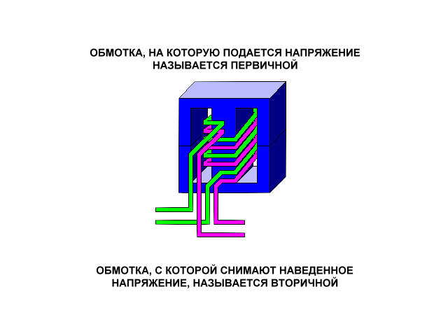
- Analog, the main element of which is a step-down transformer, in addition to its main function, it also provides galvanic isolation.
- Impulse principle.
Let's look at how these two options differ.
PSU based on a power transformer
Let's consider a simplified block diagram of this device. As can be seen from the figure, a step-down transformer is installed at the input, with its help the amplitude of the supply voltage is converted, for example, from 220 V we get 15 V. The next block is a rectifier, its task is to convert the sinusoidal current into a pulsed one (the harmonic is shown above the symbolic image). For this purpose, rectifying semiconductor elements (diodes) connected via a bridge circuit are used. Their operating principle can be found on our website.
The next block performs two functions: it smoothes the voltage (a capacitor of appropriate capacity is used for this purpose) and stabilizes it. The latter is necessary so that the voltage does not “drop” when the load increases.
The given block diagram is greatly simplified; as a rule, a source of this type has an input filter and protective circuits, but this is not important for explaining the operation of the device.
All the disadvantages of the above option are directly or indirectly related to the main design element - the transformer. Firstly, its weight and dimensions limit miniaturization. In order not to be unfounded, we will use as an example a step-down transformer 220/12 V with a rated power of 250 W. The weight of such a unit is about 4 kilograms, dimensions 125x124x89 mm. You can imagine how much a laptop charger based on it would weigh.
Secondly, the price of such devices is sometimes many times higher than the total cost of the other components.
Pulse devices
As can be seen from the block diagram shown in Figure 3, the operating principle of these devices differs significantly from analog converters, primarily in the absence of an input step-down transformer.
 Figure 3. Block diagram of a switching power supply
 Let's consider the operating algorithm of such a source:
- Power is supplied to the network filter; its task is to minimize network noise, both incoming and outgoing, that arises as a result of operation.
- Next, the unit for converting sinusoidal voltage into pulsed constant voltage and a smoothing filter come into operation.
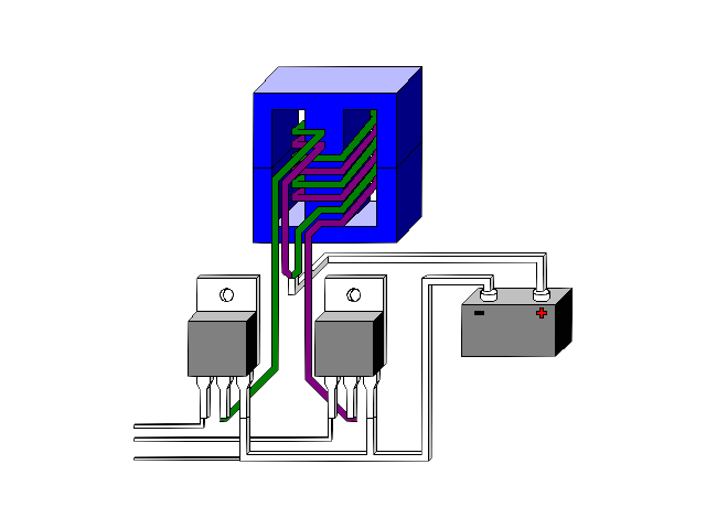
- At the next stage, an inverter is connected to the process; its task is related to the formation of rectangular high-frequency signals. Feedback with the inverter is carried out through the control unit.
- The next block is IT, it is necessary for automatic generator mode, supplying voltage to the circuit, protection, controller control, as well as the load. In addition, the IT task includes ensuring galvanic isolation between high and low voltage circuits.
Unlike a step-down transformer, the core of this device is made of ferrimagnetic materials, this contributes to the reliable transmission of RF signals, which can be in the range of 20-100 kHz. A characteristic feature of IT is that when connecting it, the inclusion of the beginning and end of the windings is critical. The small dimensions of this device make it possible to produce miniature devices; an example is the electronic harness (ballast) of an LED or energy-saving lamp.

- Next, the output rectifier comes into operation, since it works with high-frequency voltage; the process requires high-speed semiconductor elements, so Schottky diodes are used for this purpose.
- At the final phase, smoothing is performed on an advantageous filter, after which voltage is applied to the load.
Now, as promised, let’s look at the operating principle of the main element of this device – the inverter.
How does an inverter work?
RF modulation can be done in three ways:
- pulse-frequency;
- phase-pulse;
- pulse width.
In practice, the last option is used. This is due both to the simplicity of implementation and to the fact that PWM has a constant communication frequency, unlike the other two modulation methods. A block diagram describing the operation of the controller is shown below.
The operating algorithm of the device is as follows:
The reference frequency generator generates a series of rectangular signals, the frequency of which corresponds to the reference one. Based on this signal, a sawtooth U P is formed, which is supplied to the input of the comparator K PWM. The UUS signal coming from the control amplifier is supplied to the second input of this device. The signal generated by this amplifier corresponds to the proportional difference between U P (reference voltage) and U RS (control signal from the feedback circuit). That is, the control signal UUS is, in fact, a mismatch voltage with a level that depends on both the current on the load and the voltage on it (U OUT).
This implementation method allows you to organize a closed circuit that allows you to control the output voltage, that is, in fact, we are talking about a linear-discrete functional unit. Pulses are generated at its output, with a duration depending on the difference between the reference and control signals. Based on it, a voltage is created to control the key transistor of the inverter.
The process of stabilizing the output voltage is carried out by monitoring its level; when it changes, the voltage of the control signal U PC changes proportionally, which leads to an increase or decrease in the duration between pulses.
As a result, the power of the secondary circuits changes, which ensures stabilization of the output voltage.
To ensure safety, galvanic isolation between the power supply and feedback is required. As a rule, optocouplers are used for this purpose.
Strengths and weaknesses of pulsed sources
If we compare analog and pulse devices of the same power, the latter will have the following advantages:
- Small size and weight due to the absence of a low-frequency step-down transformer and control elements that require heat removal using large radiators. Thanks to the use of high-frequency signal conversion technology, it is possible to reduce the capacitance of the capacitors used in the filters, which allows the installation of smaller elements.
- More high efficiency, since the main losses are caused only by transient processes, while in analog circuits a lot of energy is constantly lost during electromagnetic conversion. The result speaks for itself, increasing efficiency to 95-98%.
- Lower cost due to the use of less powerful semiconductor elements.
- Wider input voltage range. This type of equipment is not demanding in terms of frequency and amplitude; therefore, connection to networks of various standards is allowed.
- Availability of reliable protection against short circuits, overload and other emergency situations.
The disadvantages of pulse technology include:
The presence of RF interference is a consequence of the operation of the high-frequency converter. This factor requires the installation of a filter that suppresses interference. Unfortunately, its operation is not always effective, which imposes some restrictions on the use of devices of this type in high-precision equipment.
Special requirements for the load, it should not be reduced or increased. As soon as the current level exceeds the upper or lower threshold, the output voltage characteristics will begin to differ significantly from the standard ones. As a rule, manufacturers (even recently Chinese ones) provide for such situations and install appropriate protection in their products.
Scope of application
Almost all modern electronics are powered from blocks of this type, as an example:


Assembling a switching power supply with your own hands
Let's consider the circuit of a simple power supply, where the above-described principle of operation is applied.

Designations:
- Resistors: R1 – 100 Ohm, R2 – from 150 kOhm to 300 kOhm (selectable), R3 – 1 kOhm.
- Capacities: C1 and C2 – 0.01 µF x 630 V, C3 -22 µF x 450 V, C4 – 0.22 µF x 400 V, C5 – 6800-15000 pF (selectable), 012 µF, C6 – 10 µF x 50 V, C7 – 220 µF x 25 V, C8 – 22 µF x 25 V.
- Diodes: VD1-4 - KD258V, VD5 and VD7 - KD510A, VD6 - KS156A, VD8-11 - KD258A.
- Transistor VT1 – KT872A.
- Voltage stabilizer D1 - microcircuit KR142 with index EH5 - EH8 (depending on the required output voltage).
- Transformer T1 - a w-shaped ferrite core with dimensions 5x5 is used. The primary winding is wound with 600 turns of wire Ø 0.1 mm, the secondary (pins 3-4) contains 44 turns Ø 0.25 mm, and the last winding contains 5 turns Ø 0.1 mm.
- Fuse FU1 – 0.25A.
The setup comes down to selecting the values of R2 and C5, which ensure excitation of the generator at an input voltage of 185-240 V.
Or create a winding, you can assemble a switching type power supply with your own hands, which requires a transformer with only a few turns.
In this case, a small number of parts are required, and the work can be completed in 1 hour. In this case, the IR2151 chip is used as the basis for the power supply.
For work you will need the following materials and parts:
- PTC thermistor any type.
- Pair of capacitors, which are selected with the calculation of 1 μF. at 1 W. When creating the design, we select capacitors so that they draw 220 W.
- Diode assembly"vertical" type.
- Drivers type IR2152, IR2153, IR2153D.
- Field effect transistors type IRF740, IRF840. You can choose others if they have a good resistance indicator.
- Transformer can be taken from old computer system units.
- Diodes, installed at the outlet, it is recommended to take from the HER family.
In addition, you will need the following tools:
- Soldering iron and consumables.
- Screwdriver and pliers.
- Tweezers.
Also, do not forget about the need for good lighting at the work site.
Step-by-step instruction
 circuit diagram
  structural scheme
 Assembly is carried out according to the drawn circuit diagram. The microcircuit was selected according to the characteristics of the circuit.
Assembly is carried out as follows:
- At the entrance install a PTC thermistor and diode bridges.
- Then, a pair of capacitors is installed.
- Drivers necessary to regulate the operation of valves field effect transistors. If drivers have a D index at the end of the marking, there is no need to install FR107.
- Field effect transistors installed without shorting the flanges. When attaching to the radiator, use special insulating gaskets and washers.
- Transformers installed with shorted leads.
- The output is diodes.
All elements are installed in the designated places on the board and soldered on the reverse side.
Examination
 In order to correctly assemble the power supply, you need to be careful about installing the polar elements, and you should also be careful when working with mains voltage. After disconnecting the unit from the power source, there should be no dangerous voltage remaining in the circuit. If assembled correctly, no further adjustment is required.
You can check the correct operation of the power supply as follows:
- Include in the chain at the output of the light bulb, for example, 12 volts. At the first short-term start, the light should be on. In addition, you should pay attention to the fact that all elements should not heat up. If something gets hot, it means the circuit is assembled incorrectly.
- At the second start We measure the current value using a tester. Let the unit operate for a sufficient amount of time to ensure that there are no heating elements.
In addition, it would be useful to check all elements using a tester for the presence of high current after turning off the power.
- As previously noted, the operation of a switching power supply is based on feedback. The considered circuit does not require a special organization of feedback and various power filters.
- Particular attention should be paid to the selection of field-effect transistors. In this case, IR FETs are recommended because they are renowned for their thermal resolution. According to the manufacturer, they can operate stably up to 150 degrees Celsius. However, in this circuit they do not heat up very much, which can be called a very important feature.
- If the transistors heat up constantly, active cooling should be installed. As a rule, it is represented by a fan.
Advantages and disadvantages

The pulse converter has the following advantages:
- High rate stabilization coefficient allows you to provide power conditions that will not harm sensitive electronics.
- Designs considered have a high efficiency rate. Modern versions have this figure at 98%. This is due to the fact that losses are reduced to a minimum, as evidenced by the low heating of the block.
- Large input voltage range- one of the qualities due to which such a design has spread. At the same time, the efficiency does not depend on the input current indicators. It is the immunity to the current voltage indicator that allows you to extend the service life of electronics, since jumps in the voltage indicator are a common occurrence in the domestic power supply network.
- Input frequency affects the operation of only the input elements of the structure.
- Small dimensions and weight, are also responsible for their popularity due to the proliferation of portable and portable equipment. After all, when using a linear block, the weight and dimensions increase several times.
- Organization of remote control.
- Less cost.
There are also disadvantages:
- Availability impulse interference.
- Necessity inclusion in the circuit of power factor compensators.
- Complexity self-regulation.
- Less reliable due to the complexity of the chain.
- Severe consequences when one or more circuit elements fail.
When creating such a design yourself, you should take into account that mistakes made can lead to failure of the electrical consumer. Therefore, it is necessary to provide protection in the system.
Design and operating features

When considering the operating features of the pulse unit, the following can be noted:
- At first The input voltage is rectified.
- Rectified voltage depending on the purpose and features of the entire structure, it is redirected in the form of a high-frequency rectangular pulse and fed to an installed transformer or filter operating at low frequencies.
- Transformers are small in size and weight when using a pulse unit due to the fact that increasing the frequency makes it possible to increase the efficiency of their operation, as well as reduce the thickness of the core. In addition, ferromagnetic material can be used in the manufacture of the core. At low frequency, only electrical steel can be used.
- Voltage stabilization occurs through negative feedback. Thanks to the use this method, the voltage supplied to the consumer remains unchanged, despite fluctuations in the incoming voltage and the generated load.
Feedback can be organized as follows:
- With galvanic isolation, an optocoupler or transformer winding output is used.
- If you don't need to create a junction, a resistor voltage divider is used.
Using similar methods, the output voltage is maintained with the required parameters.
Standard blocks switching power supply, which can be used, for example, to regulate the output voltage when powering , consists of the following elements:
- Input part, high voltage. It is usually represented by a pulse generator. Pulse width is the main indicator that affects the output current: the wider the indicator, the greater the voltage, and vice versa. The pulse transformer stands at the section between the input and output parts and separates the pulse.
- There is a PTC thermistor at the output part. It is made of semiconductor and has a positive temperature coefficient. This feature means that when the temperature of the element increases above a certain value, the resistance indicator increases significantly. Used as a key security mechanism.
- Low voltage part. The pulse is removed from the low-voltage winding, rectification occurs using a diode, and the capacitor acts as a filter element. The diode assembly can rectify current up to 10A. It should be taken into account that capacitors can be designed for different loads. The capacitor removes the remaining pulse peaks.
- Drivers they suppress the resistance that arises in the power circuit. During operation, drivers alternately open the gates of installed transistors. Work occurs at a certain frequency
- Field effect transistors selected taking into account resistance indicators and maximum voltage when open. At a minimum value, the resistance significantly increases efficiency and reduces heating during operation.
- Transformer standard for downgrade.
Taking into account the chosen circuit, you can begin to create a power supply of the type in question.
THIS MATERIAL CONTAINS A LARGE NUMBER OF ANIMATED APPLICATIONS!!!
For the Microsoft Internet Extlorer browser, you need to temporarily disable some functions, namely:
- turn off integrated bars from Yandex, Google, etc.
- turn off the status bar (uncheck it):
Turn off the address bar:

If desired, you can turn off the REGULAR BUTTONS, but the resulting screen area is already enough

Otherwise, you don’t need to make any other adjustments - the material is controlled using buttons built into the material, and you can always return the removed panels to their place.
ELECTRICITY CONVERSION
Before we begin to describe the operating principle of switching power supplies, we should recall some details from the general physics course, namely what electricity is, what a magnetic field is and how they depend on each other.
We will not delve too deeply and we will also keep silent about the reasons for the appearance of electricity in various objects - for this you just need to stupidly retype 1/4 of the physics course, so we hope that the reader knows what electricity is not from the inscriptions on the signs "DO NOT CLIMB - WILL KILL !". However, to begin with, let us recall what it happens to be, this is electricity itself, or rather voltage.

Well, now, purely theoretically, suppose that we have a conductor as a load, i.e. the most common piece of wire. What happens in it when current flows through it is clearly shown in the following figure:

If everything is clear with the conductor and the magnetic field around it, then we will fold the conductor not into a ring, but into several rings, so that our inductor will show itself more actively and see what happens next.

At this very place, it makes sense to drink tea and let the brain absorb what you just learned. If the brain is not tired, or this information already known, then look further
Bipolar transistors, field-effect transistors (MOSFETs) and IGBTs are used as power transistors in switching power supplies. Only the device manufacturer decides which power transistor to use, since both of them have their own advantages and disadvantages. However, it would be unfair not to note that bipolar transistors are practically not used in powerful power supplies. MOSFET transistors are best used at conversion frequencies from 30 kHz to 100 kHz, but IGBTs “like lower frequencies - it is better not to use above 30 kHz.
Bipolar transistors are good because they close quite quickly, since the collector current depends on the base current, but in the open state they have a fairly high resistance, which means that there will be a fairly large voltage drop across them, which definitely leads to unnecessary heating of the transistor itself .
Field valves have very little active resistance in the open state, which does not cause a large release of heat. However, the more powerful the transistor, the greater its gate capacitance, and rather large currents are required to charge and discharge it. This dependence of the gate capacitance on the power of the transistor is due to the fact that the field-effect transistors used for power supplies are manufactured using MOSFET technology, the essence of which is the use of parallel connection of several field-effect transistors with an insulated gate and made on a single chip. And the more powerful the transistor, the more parallel transistors are used and the gate capacitances are summed up.
An attempt to find a compromise are transistors made using IGBT technology, since they are constituent elements. Rumor has it that they turned out purely by accident, when trying to repeat the MOSFET, but instead of field-effect transistors, they turned out not quite field and not quite bipolar. The control electrode is the gate of a low-power field-effect transistor built inside, which, with its source-drain, already controls the base current of powerful bipolar transistors connected in parallel and made on one crystal of a given transistor. This results in a fairly small gate capacitance and not a very high active resistance in the open state.
There are not so many basic circuits for connecting the power part:
AUTO-GENERATOR POWER UNITS. A positive connection is used, usually inductive. The simplicity of such power supplies imposes some restrictions on them - such power supplies “love” a constant, unchanging load, since the load affects the feedback parameters. Such sources come in both single-cycle and push-pull types.
FORCED EXCITATION PULSE POWER SUPPLY. These power supplies are also divided into single-cycle and push-pull. The former, although they are more loyal to changing loads, still do not very consistently maintain the required power reserve. And audio equipment has a fairly large spread in consumption - in pause mode the amplifier consumes a few watts (the quiescent current of the final stage), and at audio signal peaks the consumption can reach tens or even hundreds of watts.
Thus, the only, most acceptable option for a switching power supply for audio equipment is the use of push-pull circuits with forced excitation. Also, do not forget that during high-frequency conversion it is necessary to pay more careful attention to filtering the secondary voltage, since the appearance of power supply noise in the audio range will negate all efforts in manufacturing pulse source power supply for the power amplifier. For the same reason, the conversion frequency is moved further away from the audio range. The most popular conversion frequency used to be around 40 kHz, but modern element base allows conversion at much higher frequencies - up to 100 kHz.
There are two basic types of these pulsed sources - stabilized and unstabilized.
Stabilized power supplies use pulse-width modulation, the essence of which is to shape the output voltage by adjusting the duration of the voltage supplied to the primary winding, and compensation for the absence of pulses is carried out by LC circuits connected at the secondary power output. The big advantage of stabilized power supplies is the stability of the output voltage, which does not depend on the input voltage of the 220 V network or on the power consumption.
Non-stabilized ones simply control the power part with a constant frequency and pulse duration and differ from a conventional transformer only in size and much smaller capacitances of the secondary supply capacitors. The output voltage directly depends on the 220 V network, and has a slight dependence on the power consumption (at idle the voltage is slightly higher than the calculated one).
The most popular power circuits of switching power supplies are:
With midpoint(PUSH-PULL). They are usually used in low-voltage power supplies, since they have some peculiarities in the requirements for the element base. The power range is quite large.
Half bridges. The most popular circuit in network switching power supplies. Power range up to 3000 W. A further increase in power is possible, but the cost reaches the level of the bridge version, so it is somewhat uneconomical.
Pavements. This scheme is not economical at low powers, since it contains twice the number of power switches. Therefore, it is most often used at powers above 2000 W. Maximum powers are within 10,000 W. This circuitry is basic in the manufacture of welding machines.
Let's take a closer look at who is who and how they work.
WITH MIDDLE POINT
As has been shown, this power circuit design is not recommended for use in creating network power supplies, but NOT RECOMMENDED does not mean NOT possible. It is simply necessary to take a more careful approach to the selection of the element base and the manufacture of the power transformer, as well as take into account fairly high voltages when laying out the printed circuit board.
This power stage has gained maximum popularity in car audio equipment, as well as in uninterruptible power supplies. However, in this field, this circuitry suffers from some inconveniences, namely the limitation of maximum power. And the point is not in the element base - today MOSFET transistors with instantaneous drain-source current values of 50-100 A are not at all in short supply. The point is in the overall power of the transformer itself, or rather in the primary winding.
The problem is... However, to be more convincing, we will use a program for calculating the winding data of high-frequency transformers.
Let's take 5 rings of standard size K45x28x8 with a permeability of M2000HM1-A, set a conversion frequency of 54 kHz and a primary winding of 24 V (two half-windings of 12 V each). As a result, we find that this core can develop a power of 658 W, but the primary winding must contain 5 turns , i.e. 2.5 turns per half winding. Somehow it’s not naturally enough... However, if you raise the conversion frequency to 88 kHz, you get only 2 (!) turns per half-winding, although the power looks very tempting - 1000 W.
It seems that you can come to terms with such results and distribute 2 turns evenly throughout the entire ring, too, if you try hard, you can, but the quality of the ferrite leaves much to be desired, and the M2000HM1-A at frequencies above 60 kHz already heats up quite a bit, well at 90 kHz it is already necessary to blow it.
So whatever you say, it turns out to be a vicious circle - by increasing the dimensions to obtain more power, we reduce the number of turns of the primary winding too much; by increasing the frequency, we again reduce the number of turns of the primary winding, but in addition we get extra heat.
It is for this reason that dual converters are used to obtain powers above 600 W - one control module issues control pulses to two identical power modules containing two power transformers. The output voltages of both transformers are summed. It is in this way that the power supply for heavy-duty factory-produced car amplifiers is organized and about 500..700 W and no more are removed from one power module. There are several ways of summing:
- summation of alternating voltage. The current is supplied synchronously to the primary windings of the transformers, therefore the output voltages are synchronous and can be connected in series. It is not recommended to connect the secondary windings in parallel from two transformers - a small difference in winding or quality of ferrite leads to large losses and reduced reliability.
- summation after rectifiers, i.e. constant voltage. The best option is that one power module produces positive voltage for the power amplifier, and the second - negative.
- generation of power supply for amplifiers with two-level power supply by adding two identical bipolar voltages.
HALF BRIDGE

The half-bridge circuit has quite a lot of advantages - it is simple, therefore reliable, easy to replicate, does not contain scarce parts, and can be implemented on both bipolar and hollow-point transistors. IGBT transistors also work perfectly in it. However, she does have a weak point. These are pass-through capacitors. The fact is that at high powers a fairly large current flows through them and the quality of the finished switching power supply directly depends on the quality of this particular component.
But the problem is that the capacitors are constantly being recharged, therefore they must have a minimum TERMINAL-PLATE resistance, since with a high resistance, quite a lot of heat will be generated in this area and in the end the terminal will simply burn off. Therefore, it is necessary to use film capacitors as pass-through capacitors, and the capacitance of one capacitor can reach a capacity of 4.7 μF in extreme cases, if one capacitor is used - a circuit with one capacitor is also quite often used, according to the principle of the UMZCH output stage with unipolar power supply. If two 4.7 μF capacitors are used (their connection point is connected to the transformer winding, and the free leads are connected to the positive and negative power buses), then this configuration is quite suitable for powering power amplifiers - the total capacitance for AC voltage The transformation adds up and the result is equal to 4.7 µF + 4.7 µF = 9.4 µF. However, this option is not designed for long-term continuous use with maximum load - it is necessary to divide the total capacitance into several capacitors.
If it is necessary to obtain large capacitances (low conversion frequency), it is better to use several capacitors of smaller capacity (for example, 5 pieces of 1 μF connected in parallel). However, a large number of capacitors connected in parallel quite significantly increases the dimensions of the device, and the total cost of all the garlands of capacitors is not small. Therefore, if you need to get more power, it makes sense to use a bridge circuit.
For the half-bridge version, powers above 3000 W are not desirable - boards with pass-through capacitors will be too bulky. Using electrolytic capacitors as pass-through capacitors makes sense, but only at powers up to 1000 W, since at high frequencies electrolytes are not effective and begin to heat up. Paper capacitors have shown themselves to be very good as pass-through capacitors, but their dimensions...
For greater clarity, we provide a table of the dependence of the capacitor reactance on frequency and capacitance (Ohm):
| Capacitor capacity |
Conversion frequency |
|||||||
Just in case, we remind you that when using two capacitors (one for plus, the other for minus), the final capacitance will be equal to the sum of the capacitances of these capacitors. The resulting resistance does not generate heat, since it is reactive, but it can affect the efficiency of the power supply at maximum loads - the output voltage will begin to decrease, despite the fact that the overall power of the power transformer is quite sufficient.
BRIDGE

The bridge circuit is suitable for any power, but is most effective at high powers (for network power supplies this is power from 2000 W). The circuit contains two pairs of power transistors controlled synchronously, but the need for galvanic isolation of the emitters of the upper pair introduces some inconvenience. However, this problem is completely solvable when using control transformers or specialized microcircuits, for example, for field-effect transistors, you can fully use IR2110 - a specialized development from International Rectifier.
However, the power part has no meaning if it is not controlled by the control module.
Specialized microcircuits There are quite a lot of devices capable of controlling the power part of switching power supplies, but the most successful development in this area is the TL494, which appeared in the last century, but nevertheless has not lost its relevance, since it contains ALL the necessary components for controlling the power part of switching power supplies. The popularity of this microcircuit is primarily evidenced by its release by several large manufacturers of electronic components.
Let's consider the principle of operation of this microcircuit, which full responsibility can be called a controller, since it has ALL the necessary nodes.


PART II
What exactly is the PWM method of voltage regulation?
The method is based on the same inertia of inductance, i.e. its inability to instantly pass current. Therefore, by adjusting the duration of the pulses, you can change the final constant voltage. Moreover, for switching power supplies it is better to do this in the primary circuits and thus save money on creating a power supply, since this source will play two roles at once:
- voltage conversion;
- stabilization of the output voltage.
Moreover, much less heat will be generated in this case compared to a linear stabilizer installed at the output of a non-stabilized switching power supply.
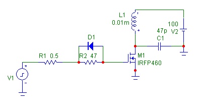
For more clarity, you should look at the figure below:
![]()
The figure shows an equivalent circuit pulse stabilizer in which the generator of rectangular pulses V1 acts as a power key, and R1 as a load. As can be seen from the figure, with a fixed amplitude of the output pulses of 50 V, by changing the duration of the pulses, it is possible to change the applied to load voltage, and with very small thermal losses, depending only on the parameters of the power switch used.
We figured out the operating principles of the power unit, as well as the controls. All that remains is to connect both nodes and get a ready-made switching power supply.
The load capacity of the TL494 controller is not very large, although it is enough to control one pair of power transistors of the IRFZ44 type. However, for more powerful transistors, current amplifiers are already needed that can develop the required current at the control electrodes of power transistors. Since we are trying to reduce the size of the power supply and move away from the audio range, MOSFETs will be the best use as power transistors.

Variants of structures in the manufacture of MOSFETs.
On the one hand, large currents are not needed to control a field-effect transistor - they are opened by voltage. However, there is a fly in the ointment in this barrel of honey, in this case, which consists in the fact that although the gate has a huge active resistance that does not consume current to drive the transistor, the gate has a capacitance. And for its charge and discharge, large currents are just needed, since at high conversion frequencies, the reactance is already reduced to limits that cannot be ignored. And the greater the power of the power MOSFET transistor, the greater the capacitance of its gate.
For example, take the IRF740 (400 V, 10A) which has a gate capacitance of 1400 pF and the IRFP460 (500 V, 20 A) which has a gate capacitance of 4200 pF. Since both the first and the second gate voltage should not exceed ± 20 V, then we take a voltage of 15 V as control pulses and see in the simulator what happens at a generator frequency of 100 kHz on resistors R1 and R2, which are connected in series with capacitors at 1400 pF and 4200 pF.

Test stand.
When a current flows through an active load, a voltage drop forms on it; by this value, one can judge the instantaneous values of the flowing current.

Drop across resistor R1.
As can be seen from the figure, immediately upon the appearance of a control pulse, approximately 10.7 V drops across the resistor R1. With a resistance of 10 ohms, this means that the instantaneous current value reaches 1, A (!). As soon as the pulse ends on the resistor R1, 10.7 V also drops, therefore, in order to discharge the capacitor C1, a current of about 1 A is required ..
To charge and discharge a 4200 pF capacitance through a 10 ohm resistor, 1.3 A is required, since 13.4 V drops across the 10 ohm resistor.

The conclusion suggests itself - for charging and discharging gate capacitances, it is necessary that the helmet operating the gates of power transistors can withstand fairly large currents, despite the fact that the total consumption is quite small.
To limit instantaneous current values in the gates of field-effect transistors, current-limiting resistors from 33 to 100 Ohms are usually used. An excessive decrease in these resistors increases the instantaneous value of the flowing currents, and an increase increases the duration of operation of the power transistor in linear mode, which leads to unreasonable heating of the latter.
Quite often a chain is used consisting of a resistor and a diode connected in parallel. This trick is used primarily to relieve the control stage during charging and speed up the discharge of the gate capacitance.
Fragment of a single-cycle converter.
In this way, not an instantaneous appearance of current in the winding of the power transformer is achieved, but a somewhat linear one. Although this increases the temperature of the power stage, it quite significantly reduces the self-induction surges that inevitably appear when a rectangular voltage is applied to the transformer winding.

Self-inductance in the operation of a single-ended converter
(red line - voltage on the transformer winding, blue - supply voltage, green - control pulses).
So we’ve sorted out the theoretical part and we can draw some conclusions:
To create a switching power supply, you need a transformer whose core is made of ferrite;
To stabilize the output voltage of a switching power supply, a PWM method is required, which the TL494 controller can handle quite successfully;
The power section with a midpoint is most convenient for low-voltage switching power supplies;
The power part of half-bridge circuitry is convenient for low and medium powers, and its parameters and reliability largely depend on the quantity and quality of pass-through capacitors;
The bridge type power section is more advantageous for high powers;
When using MOSFETs in the power part, do not forget about the gate capacitance and calculate the control elements of power transistors adjusted for this capacitance;
Since we’ve sorted out the individual components, let’s move on to the final version of the switching power supply. Since both the algorithm and circuitry of all half-bridge sources are almost the same, to explain which element is needed for what, we will break down the most popular one, with a power of 400 W, with two bipolar output voltages.

It remains to note some new features:
Resistors R23, R25, R33, R34 serve to create an RC filter, which is highly desirable when using electrolytic capacitors at the output of pulsed sources. Ideally, of course, it is better to use LC filters, but since the “consumers” are not very powerful, you can completely get by with an RC filter. The resistance of these resistors can be used from 15 to 47 Ohms. R23 is better with a power of 1 W, the rest at 0.5 W are quite enough.
C25 and R28 - snubber that reduces self-induction emissions in the winding of a power transformer. They are most effective at capacitances above 1000 pF, but in this case too much heat is generated at the resistor. Necessary in the case when there are no chokes after the rectifier diodes of the secondary power supply (the vast majority of factory equipment). If chokes are used, the effectiveness of snubbers is not so noticeable. Therefore, we install them extremely rarely and the power supplies do not work worse because of this.
If some element values differ on the board and circuit diagram, these values are not critical - you can use both.
If there are elements on the board that are not on the circuit diagram (usually these are power supply capacitors), then you can not install them, although it will be better with them. If you decide to install, then you can use not electrolytic capacitors of 0.1...0.47 μF, but electrolytic capacitors of the same capacity as those that are connected in parallel with them.
On the board OPTION 2 Near the radiators there is a rectangular part that is drilled around the perimeter and power supply control buttons (on-off) are installed on it. The need for this hole is due to the fact that the 80 mm fan does not fit in height in order to secure it to the radiator. Therefore, the fan is installed below the base of the printed circuit board.
SELF ASSEMBLY INSTRUCTIONS
STABILIZED PULSE POWER SUPPLY
To begin with, you should carefully read the circuit diagram, but this should always be done before starting assembly. This voltage converter operates in a half-bridge circuit. How it differs from the others is described in detail.

The circuit diagram is packaged in WinRAR of the old version and is executed on a WORD-2000 page, so there should be no problems with printing this page. Here we will look at it in fragments, since we want to maintain high readability of the diagram, but it does not fit entirely correctly on the monitor screen. Just in case, you can use this drawing to present the picture as a whole, but it’s better to print it out...
Figure 1 shows a filter and a mains voltage rectifier. The filter is designed primarily to prevent the penetration of impulse noise from the converter into the network. Completed on L-C basis. A ferrite core of any shape is used as inductance (rod ones are better not needed - there is a large background from them) with a wound single winding. The dimensions of the core depend on the power of the power source, since the more powerful the source, the more interference it will create and the better the filter needed.

Picture 1.
The approximate dimensions of the cores, depending on the power of the power source, are summarized in Table 1. The winding is wound until the core is filled, the diameter(s) of the wire should be selected at the rate of 4-5 A/mm sq.
| Table 1 | ||||
|
POWER SUPPLY POWER |
RING CORE |
W-SHAPED CORE |
||
|
Diameter from 22 to 30 with a thickness of 6-8 mm |
Width from 24 to 30 with thickness 6-8 mm |
|||
|
Diameter from 32 to 40 with a thickness of 8-10 mm |
Width from 30 to 40 with a thickness of 8-10 mm |
|||
|
Diameter from 40 to 45 with a thickness of 8-10 mm |
Width from 40 to 45 with a thickness of 8-10 mm |
|||
|
Diameter from 40 to 45 with a thickness of 10-12 mm |
Width from 40 to 45 with thickness 10-12 mm |
|||
|
Diameter from 40 to 45 with a thickness of 12-16 mm |
Width from 40 to 45 with thickness 12-16 mm |
|||
|
Diameter from 40 to 45 with a thickness of 16-20 mm |
Width from 40 to 45 with thickness 16-20 mm |
|||
Here we should explain a little why the diameter (s) and what 4-5 A/mm sq is.
This category of power supplies belongs to high-frequency. Now let's remember the physics course, namely the place where it is said that at high frequencies the current flows not across the entire cross-section of the conductor, but along its surface. And the higher the frequency, the larger part of the conductor cross-section remains unused. For this reason, in pulsed high-frequency devices, the windings are made using bundles, i.e. Several thinner conductors are taken and folded together. Then the resulting bundle is twisted slightly along the axis so that individual conductors do not stick out in different directions during winding, and the windings are wound with this bundle.
4-5 A/mm kV means that the voltage in the conductor can reach four to five Amperes per square millimeter. This parameter is responsible for heating the conductor due to the voltage drop in it, because the conductor has, although not large, resistance. In pulse technology, winding products (chokes, transformers) have relatively small dimensions, therefore they will be cooled well, so the voltage can be used exactly 4-5 A/mm sq. But for traditional transformers made on iron, this parameter should not exceed 2.5-3 A/mm sq. The diameter plate will help you calculate how many wires and what cross-section. In addition, the plate will tell you what power can be obtained by using a particular number of wires of the available wire, if you use it as the primary winding of a power transformer. Open the sign.
The capacitance of capacitor C4 must be at least 0.1 µF, if it is used at all. Voltage 400-630 V. Formulation if it is used at all It is not used in vain - the main filter is inductor L1, and its inductance is quite large and the probability of penetration of RF interference is reduced to almost zero values.
The VD diode bridge is used to rectify alternating mains voltage. An RS type assembly (end terminals) is used as a diode bridge. For a power of 400 W, you can use RS607, RS807, RS1007 (at 700 V, 6, 8 and 10 A, respectively), since the installation dimensions of these diode bridges are the same.
Capacitors C7, C8, C11 and C12 are necessary to reduce impulse noise created by diodes as the alternating voltage approaches zero. The capacitance of these capacitors is from 10 nF to 47 nF, the voltage is not lower than 630 V. However, after taking several measurements, it was found that L1 copes well with this interference, and to eliminate influence in the primary circuits, capacitor C17 is sufficient. In addition, the capacitances of capacitors C26 and C27 also contribute - for the primary voltage they are two capacitors connected in series. Since their ratings are equal, the final capacitance is divided by 2 and this capacitance not only serves to operate the power transformer, but also suppresses impulse noise in the primary power supply. Based on this, we refused to use C7, C8, C11 and C12, but if someone really wants to install them, then there is enough space on the board, on the side of the tracks.
The next fragment of the circuit is the current limiters on R8 and R11 (Figure 2). These resistors are necessary to reduce the charging current of electrolytic capacitors C15 and C16. This measure is necessary because at the moment of switching on a very large current is required. Neither the fuse nor the diode bridge VD are capable of withstanding such a powerful current surge, even for a short time, although the inductance L1 limits the maximum value of the flowing current, in this case this is not enough. Therefore, current-limiting resistors are used. The resistor power of 2 W was chosen not so much because of the heat generated, but because of the rather wide resistive layer that can briefly withstand a current of 5-10 A. For power supplies with a power of up to 600 W, you can use resistors with a power of 1 W, or use one resistor power of 2 W, you only need to meet the condition - the total resistance of this circuit should not be less than 150 Ohms and should not be more than 480 Ohms. If the resistance is too low, the chance of destruction of the resistive layer increases, if it is too high, the charging time of C15, C16 increases and the voltage on them will not have time to approach the maximum value before relay K1 will operate and the contacts of this relay will have to switch too much current. If wirewound resistors are used instead of MLT resistors, the total resistance can be reduced to 47...68 Ohms.
The capacity of capacitors C15 and C16 is also selected depending on the power of the source. You can calculate the required capacity using a simple formula: PER ONE WATT OF OUTPUT POWER, 1 μF OF PRIMARY POWER FILTER CAPACITORS IS REQUIRED. If you have doubts about your mathematical abilities, you can use the table, in which you simply put the power of the power source that you are going to make and see how many and what capacitors you need. Please note that the board is designed for installation of network electrolytic capacitors with a diameter of 30 mm.
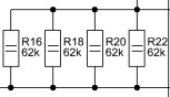
Figure 3
Figure 3 shows quenching resistors whose main purpose is to form the starting voltage. The power is not lower than 2 W, they are installed on the board in pairs, one above the other. Resistance from 43 kOhm to 75 kOhm. It is VERY desirable that ALL resistors be of the same value - in this case the heat is distributed evenly. For low powers, a small relay with low consumption is used, so you can get by with 2 or three quenching resistors. They are installed on the board one above the other.

Figure 4
Figure 4 - power supply stabilizer for the control module - in any case there is an intergaral stabilizer at +15V. A radiator is required. Size... Usually a radiator from the penultimate stage of domestic amplifiers is enough. You can ask for something in TV workshops - TV boards usually have 2-3 suitable radiators. The second one is used to cool the VT4 transistor, which controls the fan speed (Figure 5 and 6). Capacitors C1 and C3 can also be used at 470 uF at 50 V, but such a replacement is only suitable for power supplies that use certain type relays whose coil resistance is quite high. On more powerful sources, a more powerful relay is used and reducing the capacitance of C1 and C3 is highly undesirable.

Figure 5 
Figure 6
Transistor VT4 - IRF640. Can be replaced with IRF510, IRF520, IRF530, IRF610, IRF620, IRF630, IRF720, IRF730, IRF740, etc. The main thing is that it must be in the TO-220 housing, have a maximum voltage of at least 40 V and a maximum current of at least 1 A.
Transistor VT1 is almost any direct transistor with a maximum current of more than 1 A, preferably with a low saturation voltage. Transistors in TO-126 and TO-220 packages perform equally well, so you can choose a lot of replacements. If you screw on a small radiator, even a KT816 will be quite suitable (Figure 7).

Figure 7
Relay K1 - TRA2 D-12VDC-S-Z or TRA3 L-12VDC-S-2Z. In fact, it is the most ordinary relay with a 12 V winding and a contact group capable of switching 5 A or more. You can use relays used in some TVs to turn on the demagnetization loop, just keep in mind that the contact group in such relays has a different pinout and even if it is installed on the board without problems, you should check which pins are closed when voltage is applied to the coil. TRA2 differs from TRA3 in that TRA2 has one contact group capable of switching current up to 16 A, and TRA3 has 2 contact groups of 5 A each.
By the way, the printed circuit board is offered in two versions, namely with and without a relay. In the version without a relay, the soft start system of the primary voltage is not used, so this option is suitable for a power source with a power of no more than 400 W, since it is highly not recommended to turn on a “direct” capacitance of more than 470 μF without current limiting. In addition, a bridge with a maximum current of 10 A MUST be used as a VD diode bridge, i.e. RS1007. Well, the role of the relay in the version without soft start is performed by the LED. The standby function is retained.
Buttons SA2 and SA3 (it is assumed that SA1 is a power switch) are buttons of any type without locking, for which you can make a separate printed circuit board, or you can attach them in another convenient way. It must be remembered that the button contacts are galvanically connected to the 220 V network, therefore, it is necessary to exclude the possibility of touching them during operation of the power source.
There are quite a few analogues of the TL494 controller, you can use any, just keep in mind that different manufacturers may have some differences in parameters. For example, when replacing one manufacturer with another, the conversion frequency may change, but not much, but the output voltage can change up to 15%.
IR2110, in principle, is not a defective driver, and it does not have many analogues - IR2113, but IR2113 has a larger number of housing options, so be careful - a DIP-14 housing is required.
When mounting a board, instead of microcircuits, it is better to use connectors for microcircuits (sockets), ideally collet connectors, but regular ones are also possible. This measure will avoid some misunderstandings, since there are quite a lot of defects among both TL494 (no output pulses, although the clock generator is working) and among IR2110 (no control pulses to the upper transistor), so the terms of the warranty should be agreed upon with the seller of the chips.
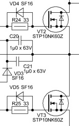
Figure 8
Figure 8 shows the power section. It is better to use fast diodes VD4...VD5, for example SF16, but in the absence of such, HER108 is also quite suitable. C20 and C21 - the total capacitance is at least 1 µF, so you can use 2 capacitors of 0.47 µF each. The voltage is at least 50 V, ideally a 1 µF 63 V film capacitor (in the event of a breakdown of the power transistors, the film capacitor remains intact, but the multilayer ceramics dies). For power supplies up to 600 W, the resistance of resistors R24 and R25 can be from 22 to 47 Ohms, since the gate capacitances of the power transistors are not very large.
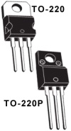
Power transistors can be any of those listed in Table 2 (TO-220 or TO-220R housing).
| table 2 | ||||||
|
Name |
Gate capacity, |
Max voltage, |
Max current, |
Thermal power |
Resistance, |
|
|
|
||||||
| If the thermal power does not exceed 40 W, then the transistor body is completely plastic and a larger heat sink is required so as not to bring the temperature of the crystal to a critical value. Gate voltage for all is no more than ±20 V |
||||||
Thyristors VS1 and VS, in principle, the brand does not matter, the main thing is that the maximum current must be at least 0.5 A and the housing must be TO-92. We use either MCR100-8 or MCR22-8.
It is advisable to choose diodes for low-current power supply (Figure 9) with a short recovery time. Diodes of the HER series, for example HER108, are quite suitable, but others can be used, for example SF16, MUR120, UF4007. Resistors R33 and R34 are 0.5 W, resistance from 15 to 47 Ohms, with R33 = R34. The service winding operating on VD9-VD10 must be designed for 20 V stabilized voltage. In the winding calculation table it is marked in red.
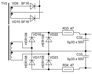
Figure 9
Power rectifier diodes can be used in both the TO-220 and TO-247 packages. In both versions of the printed circuit board, it is assumed that the diodes will be installed on top of each other and connected to the board by conductors (Figure 10). Of course, when installing diodes you should use thermal paste and insulating spacers (mica).

Figure 10
It is advisable to use diodes with a short recovery time as rectifier diodes, since the heating of the diodes at idle depends on this (the internal capacitance of the diodes is affected and they simply heat up on their own, even without load). The list of options is summarized in Table 3
| Table 3 | |||
|
Name |
Maximum voltage |
Maximum current |
Recovery time |
The current transformer performs two roles - it is used precisely as a current transformer and as an inductance connected in series with the primary winding of the power transformer, which makes it possible to slightly reduce the speed at which current appears in the primary winding, which leads to a reduction in self-induction emissions (Figure 11).

Figure 11
There are no strict formulas for calculating this transformer, but it is strongly recommended to comply with some restrictions:
| FOR POWERS FROM 200 TO 500 W - RING WITH DIAMETER 12...18 MM FOR POWER FROM 400 TO 800 W - RING WITH DIAMETER 18...26 MM FOR POWER FROM 800 TO 1800 W - RING WITH DIAMETER 22...32 MM FOR POWER FROM 1500 TO 3000 W - RING WITH DIAMETER 32...48 MM |
FERRITE RINGS, PERMEABILITY 2000, THICKNESS 6...12 MM |
NUMBER OF TURNS OF THE PRIMARY WINDING:
3 TURNINGS FOR BAD COOLING CONDITIONS AND 5 TURNINGS IF THE FAN BLOWS DIRECTLY ON THE BOARD
NUMBER OF TURNS OF THE SECONDARY WINDING:
12...14 FOR PRIMARY OF 3 TURNS AND 20...22 FOR PRIMARY OF 5 TURNS
IT IS MUCH MORE CONVENIENT TO WIND THE TRANSFORMER SECTIONALLY - THE PRIMARY WINDING DOES NOT INTERLINE WITH THE SECONDARY WINDING. IN THIS CASE, IT IS NOT DIFFICULT TO REWIND THE TURN TO THE PRIMARY WINDING. IN THE FINAL, AT A LOAD OF 60% OF THE MAXIMUM, THE UPPER TERMINAL OF R27 SHOULD BE ABOUT 12...15 V
The primary winding of the transformer is wound with the same winding as the primary winding of the TV2 power transformer, the secondary with a double wire with a diameter of 0.15...0.3 mm.
To manufacture a power transformer for a pulse power supply unit, you should use a program for calculating pulse transformers. The design of the core is not of fundamental importance - it can be toroidal or W-shaped. Printed circuit boards allow you to use both without problems. If the overall capacity of the W-shaped medium is not enough, it can also be folded into a bag like rings (Figure 12).

Figure 12
You can get hold of W-shaped ferrites in TV workshops - not often, but power transformers in TVs fail. The easiest way to find power supplies from domestic TVs is the 3rd ... 5th. Do not forget that if a transformer of two or three mediums is required, then ALL mediums must be of the same brand, i.e. for disassembly, it is necessary to use transformers of the same type.
If the power transformer is made of 2000 rings, then you can use Table 4.
|
IMPLEMENTATION |
REAL |
PARAMETER |
CONVERSION FREQUENCY |
||||||
|
MORE IS POSSIBLE |
OPTIMAL |
HIGH HEAT |
|||||||
|
1 RING |
OVERALL POWER |
||||||||
| TURNINGS PER FIRST WINDING | |||||||||
|
2 RINGS |
OVERALL POWER |
||||||||
| TURNINGS PER FIRST WINDING | |||||||||
|
1 RING |
OVERALL POWER |
||||||||
| TURNINGS PER FIRST WINDING | |||||||||
|
2 RINGS |
OVERALL POWER |
||||||||
| TURNINGS PER FIRST WINDING | |||||||||
|
3 RINGS |
OVERALL POWER |
|
|
|
|||||
| TURNINGS PER FIRST WINDING |
|
|
|
||||||
|
4 RINGS A |
OVERALL POWER |
|
|
|
|
|
|||
| TURNINGS PER FIRST WINDING |
|
|
|
|
|
||||
| THE NUMBER OF TURNINGS OF THE SECONDARY WINDING IS CALCULATED THROUGH THE PROPORTION, CONSIDERING THAT THE VOLTAGE ON THE PRIMARY WINDING IS 155 V OR USING THE TABLE ( CHANGE ONLY YELLOW CELLS) | |||||||||
Please note that voltage stabilization is carried out using PWM, therefore the output calculated voltage of the secondary windings should be at least 30% greater than you need. Optimal parameters are obtained when the calculated voltage is 50...60% greater than what needs to be stabilized. For example, you need a source with an output voltage of 50 V, therefore the secondary winding of the power transformer must be designed for an output voltage of 75...80 V. This coefficient is taken into account in the secondary winding calculation table.
The dependence of the conversion frequency on the C5 and R5 ratings is shown in the graph:

It is not recommended to use a fairly large resistance R5 - too large a magnetic field is not far away and interference is possible. Therefore, we will focus on the “average” rating of R5 of 10 kOhm. With this resistance of the frequency-setting resistor, the following conversion frequencies are obtained:
|
Parameters obtained from this manufacturer |
Conversion frequency |
||
|
|
|||

(!) Here we should say a few words about winding the transformer. Quite often there are indignations, they say when self-manufacturing the source either does not deliver the required power, or the power transistors get very hot even without a load.
Frankly speaking, we also encountered this problem using 2000 rings, but it was easier for us - the presence of measuring equipment made it possible to find out the reason for such incidents, and it turned out to be quite expected - the magnetic permeability of ferrite does not correspond to the markings. In other words, on “weak” transformers we had to unwind the primary winding, on the contrary, on “heating power transistors” we had to unwind it.
A little later we stopped using rings, but the ferrite we use was not masked at all, so we took radical measures. A transformer with the calculated number of turns of the primary winding is connected to the assembled and debugged board, and the conversion frequency is changed using a trimming resistor installed on the board (instead of R5, a 22 kOhm trimmer is installed). At the moment of switching on, the conversion frequency is set within 110 kHz and begins to decrease by rotating the trimmer resistor slider. In this way, the frequency at which the core begins to enter saturation is determined, i.e. when the power transistors start to warm up without load. If the frequency drops below 60 kHz, then the primary winding is unwound, but if the temperature begins to rise by 80 kHz, then the primary winding is unwound. In this way, the number of turns for this particular core is determined, and only after that the secondary winding is wound using the plate suggested above, and the number of turns of the primary for a particular medium is indicated on the packages.
If the quality of your core is in doubt, then it is better to make a board, test it for functionality, and only then make a power transformer using the method described above.
Throttle group stabilization. In some places there was even a suggestion that he simply couldn’t work, since constant tension was flowing through him. On the one hand, such judgments are correct - the voltage is indeed of the same polarity, which means it can be recognized as constant. However, the author of such a judgment did not take into account the fact that the voltage, although constant, is pulsating and during operation in this node there is not just one process (current flow), but many, since the inductor contains not one winding, but at least two (if the output voltage needs to be bipolar) or 4 windings if two bipolar voltages are needed (Figure 13).

It is possible to make a choke both on the ring and on the W-shaped ferrite. Dimensions of course depend on the power. For powers up to 400-500 W, a medium from a surge protector for TVs with a diagonal of 54 cm and above is sufficient (Figure 14). Core design is not critical
Figure 14
It is wound in the same way as a power transformer - from several thin conductors twisted into a bundle or glued into a tape at the rate of 4-5 A/mm sq. Theoretically, the more turns, the better, so the winding is laid until the window is filled, and immediately in 2 (if a bipolar source is needed) or 4 wires (if a source with two bipolar voltages is needed.
After the smoothing capacitors there are output chokes. There are no special requirements for them, the dimensions... The boards are designed for installation of cores from TV mains power filters. Wind until the window is filled, cross-section at the rate of 4-5 A/mm sq (Figure 15).


Figure 15
Tape was mentioned above as a winding. Here we should go into a little more detail.
What's better? Harness or tape? Both methods have their advantages and disadvantages. The easiest way to make a bundle is to stretch the required number of wires and then twist them into a bundle using a drill. However, this method increases the total length of the conductors due to internal torsion, and also does not allow achieving identical magnetic field in all conductors of the bundle, and this, although not large, is still a heat loss.
Making tape is more labor-intensive and a little more expensive, since the required number of conductors is stretched and then, using polyurethane glue (TOP-TOP, SPECIALIST, MOMENT-CRYSTAL) glued into a tape. Glue is applied to the wire in small portions - 15...20 cm of the length of the conductor and then, holding the bundle between the fingers, they rub it in, making sure that the wires fit into the tape, similar to the tape bundles used to connect disk media with motherboard IBM computers. After the glue has stuck, a new portion is applied to 15...20 cm of the length of the wires and again smoothed with your fingers until a tape is obtained. And so on along the entire length of the conductor (Figure 16).

Figure 16
After the glue has completely dried, the tape is wound onto the core, and the winding with a large number of turns (usually a smaller cross-section) is wound first, and higher-current windings are wound on top. After winding the first layer, it is necessary to “lay” the tape inside the ring using a cone-shaped peg cut from wood. The maximum diameter of the peg is equal to the internal diameter of the ring used, and the minimum is 8…10 mm. The length of the cone must be at least 20 cm and the change in diameter must be uniform. After winding the first layer, the ring is simply put on the peg and pressed with force so that the ring is quite firmly jammed on the peg. Then the ring is removed, turned over and put back on the peg with the same force. The peg must be soft enough not to damage the insulation of the winding wire, so hard wood is not suitable for this purpose. In this way, the conductors are laid strictly according to the shape of the inner diameter of the core. After winding the next layer, the wire is again “laid” using a peg, and this is done after winding each next layer.
After winding all the windings (remembering to use interwinding insulation), it is advisable to warm up the transformer to 80...90°C for 30-40 minutes (you can use a gas or electric oven in the kitchen, but you should not overheat). At this temperature, the polyurethane glue becomes elastic and again acquires adhesive properties by gluing together not only the conductors located parallel to the tape itself, but also those located on top, i.e. the layers of windings are glued together, which adds mechanical rigidity to the windings and eliminates any sound effects that sometimes occur when the conductors of a power transformer are poorly tied (Figure 17).

Figure 17
The advantage of such winding is that it obtains an identical magnetic field in all wires of the tape harness, since geometrically they are located the same in relation to magnetic field. Such a strip conductor is much easier to distribute evenly along the entire perimeter of the core, which is very important even for standard transformers, and for pulse transformers it is MANDATORY condition. Using tape, you can achieve fairly dense winding, and by increasing the access of cooling air to the turns located directly inside the winding. To do this, it is enough to divide the number of necessary wires into two and make two identical strips that will be wound on each other. This will increase the thickness of the winding, but there will be a large distance between the turns of the tape, providing air access inside the transformer.
It is best to use fluoroplastic film as interlayer insulation - it is very elastic, which compensates for the tension of one edge that occurs when winding on a ring, has a fairly high breakdown voltage, is not sensitive to temperatures up to 200 ° C and is very thin, i.e. will not take up much space in the core window. But it is not always at hand. Vinyl tape can be used, but it is sensitive to temperatures above 80°C. Fabric-based electrical tape is resistant to temperatures, but has a low breakdown voltage, so when using it, it is necessary to wind at least 2 layers.
Whatever conductor and in whatever sequence you wind the chokes and power transformer, you should remember the length of the leads
If the Chokes and the power transformer are made using ferrite rings, then do not forget that before winding the edges of the ferrite ring should be rounded, since they are quite sharp, and the ferrite material is quite durable and can damage the insulation on the winding wire. After processing, the ferrite is wrapped with fluoroplastic tape or fabric tape and the first winding is wound.
For complete identity of identical windings, the windings are wound into two wires at once (meaning two bundles at once), which after winding are connected and the beginning of one winding is connected to the end of the other.
After winding the transformer, it is necessary to remove the varnish insulation on the wires. This is the most unpleasant moment, because it is VERY labor-intensive.
First of all, it is necessary to fix the terminals on the transformer itself and prevent the individual wires of their harness from being pulled out under mechanical stress. If the harness is tape, i.e. glued and heated after winding, then it is enough to wind several turns onto the taps with the same winding wire directly next to the transformer body. If a twisted harness is used, then it must be additionally twisted at the base of the terminal and also secured by winding several turns of wire. Next, the leads are either burned with a gas torch all at once, or they are cleaned one by one using a paper cutter. If the varnish has been annealed, then after cooling the wires are protected with sandpaper and twisted.
After removing the varnish, stripping and twisting the terminal, it is necessary to protect it from oxidation, i.e. coat with rosin flux. Then the transformer is installed on the board, all terminals, except for the terminal of the primary winding connected to the power transistors, are inserted into the corresponding holes; just in case, the windings should be “ringed”. Particular attention should be paid to the phasing of the windings, i.e. for compliance of the beginning of the winding with the circuit diagram. After the transformer leads are inserted into the holes, they should be shortened so that there is 3...4 mm from the end of the lead to the printed circuit board. Then the twisted lead is “untwisted” and ACTIVE flux is placed at the soldering site, i.e. This is either quenched hydrochloric acid; a drop is taken onto the tip of a match and transferred to the soldering site. Or crystalline acetyl-salicylic acid (aspirin) is added to glycerin until a porridge-like consistency is obtained (both can be purchased at the pharmacy, in the prescription department). After this, the lead is soldered to the printed circuit board, thoroughly warming it up and ensuring that the solder is evenly distributed around ALL lead conductors. Then the lead is shortened according to the soldering height and the board is thoroughly washed with either alcohol (90% minimum), or purified gasoline, or a mixture of gasoline and solvent 647 (1:1).
FIRST TURN ON
Switching on and checking the functionality is carried out in several stages to avoid troubles that will definitely arise if there is an error in installation.
1 . To test this design, you will need a separate power supply with a bipolar voltage of ±15...20 V and a power of 15...20 W. The first switching is done by connecting the MINUS TERMINAL of the additional power source to the negative primary power bus of the converter, and the COMMON is connected to the positive terminal of capacitor C1 (Figure 18). In this way, the power supply of the control module is simulated and it is checked for functionality without a power unit. Here it is advisable to use an oscilloscope and a frequency meter, but if they are not available, then you can get by with a multimeter, preferably a dial gauge (digital ones do not adequately respond to pulsating voltages).

Figure 18
At pins 9 and 10 of the TL494 controller, a pointer device connected to measure DC voltage should show almost half the supply voltage, which indicates that there are rectangular pulses on the microcircuit
Relay K1 should work the same way.
2. If the module is working normally, then you should check the power section, but again not from high voltage, but using an additional power source (Figure 19).

Figure 19
With this sequence of checking, it is very difficult to burn anything even with serious installation errors (short circuit between board tracks, failure to solder elements) since the power of the additional unit will not be enough. After switching on, the presence of the converter output voltage is checked - of course, it will be significantly lower than the calculated one (when using an additional source of ±15V, the output voltages will be underestimated by about 10 times, since the primary power supply is not 310 V but 30 V), however, the presence of output voltages indicates that there are no errors in the power part and you can move on to the lost part of the check.
3. The first switching on from the network must be done with a current limitation, which can be a regular 40-60 W incandescent lamp, which is connected instead of a fuse. The radiators should already be installed. Thus, in case of excessive consumption for any reason, the lamp will light up, and the likelihood of failure will be minimized. If everything is normal, then adjust the output voltage with resistors R26 and check the load capacity of the source by connecting the same incandescent lamp to the output. The lamp switched on instead of the fuse should light up (the brightness depends on the output voltage, i.e., on how much power the source will supply. The output voltage is regulated by resistor R26, but you may need to select R36.
4 . The functionality is checked with the fuse in place. As a load, you can use a nichrome spiral for electric stoves with a power of 2-3 kW. Two pieces of wire are soldered to the output of the power source, first to the shoulder from which the output voltage is controlled. One wire is screwed to the end of the spiral, and a crocodile is installed on the second. Now, by reinstalling the “crocodile” along the length of the spiral, you can quickly change the load resistance (Figure 20).

Figure 20
It would be a good idea to make “stretch marks” on the spiral in places with a certain resistance, for example every 5 ohms. Connecting to the “braces” It will be known in advance what the load and what the output power is at the moment. Well, power can be calculated using Ohm’s law (used in the plate).
All this is necessary to adjust the threshold for overload protection, which should operate stably when the actual power exceeds the calculated one by 10-15%. It is also checked how stably the power source holds the load.
If the power source does not deliver the calculated power, then some kind of error has crept in during the manufacture of the transformer - see above how to calculate the turns for a real core.
All that remains is to carefully study how to make a printed circuit board, and this is And you can start assembling. The necessary drawings of the printed circuit board with the original source in LAY format are in
First
number
Second
number
Third
number
Many
tel
Tolerance
+/- %
Silver
-
-
-
10^-2
10
Golden
-
-
-
10^-1
5
Black
-
0
-
1
-
Brown
1
1
1
10
1
Red
2
2
2
10^2
2
Orange
3
3
3
10^3
-
Yellow
4
4
4
10^4
-
Green
5
5
5
10^5
0,5
Blue
6
6
6
10^6
0,25
Violet
7
7
7
10^7
0,1
Grey
8
8
8
10^8
It is an inverter system. It rectifies the alternating input voltage. Next, the direct voltage obtained as a result of the previous operation is converted into rectangular pulses with an increased frequency and a certain compression, or into pulses supplied directly to the output filter low frequencies or to a transformer.
Design features
A simple switching power supply can include small-sized transformers, which can be explained quite simply: with increasing frequency, the efficiency of the transformer increases, and the requirements for the core dimensions necessary to transmit the corresponding power are noticeably reduced. Most often, such a core is made of ferromagnetic alloys, and for those devices that operate at low frequencies, electrical steel is used.
How does the device ensure stability?
The switching power supply operates in such a way that the voltage in it is stabilized due to negative feedback. With its help, you can maintain the output voltage at approximately the same level, regardless of the magnitude of its load and fluctuations at the input. Feedback can be provided in one of several ways. If a switching power supply with galvanic isolation from the network is used, then the most common methods may be to use communication using one of the transformer windings at the output or through an optocoupler. The duty cycle of the pulses at the output of the PWM controller varies depending on the value of the feedback signal, and it depends on the output voltage. If there is no need for decoupling, then most often a simple resistive divider is used. This allows the power supply to maintain the output voltage at a stable level.

Advantages
The switching power supply has a number of advantages, especially when compared with stabilizers of similar power. The lighter weight is achieved due to the fact that as the frequency increases, it is appropriate to use small transformers, provided that their supplied power is at the same level. In linear stabilizers, the bulk is made up of heavy, powerful power transformers with low frequencies, as well as large radiators of power elements operating in linear mode. The increased conversion frequency makes it possible to greatly reduce the size of the output voltage filter. Here it is appropriate to install capacitors of smaller capacity, in comparison with rectifiers operating at industrial frequencies. The rectifier can be made using a fairly simple half-wave circuit, which completely eliminates the risk of increasing voltage ripple at the output.
Performance

A switching power supply is characterized by a significantly higher efficiency compared to stabilizers due to the fact that in the latter, losses are associated with transient processes at those moments when the main element is switched. Since the key elements are in one of the states, that is, they are on or off, we are talking about minimal energy losses.
Other advantages
Switching power supplies cost much less than stabilizers, as they use a unified element base, as well as high-power key transistors. In addition, the use of power elements of lower power is allowed here, since they operate in key mode. The reliability of power supplies is quite comparable to that of linear stabilizers. In modern office equipment, computer technology, as well as consumer electronics Switching power supplies are most often used. And linear ones at the current time have been preserved only in some areas:
As power supply elements for low-current control boards of high quality household appliances: microwave ovens, washing machines, heating boilers and water heaters;
For low-power control devices of ultra-high and high reliability, designed for long-term continuous operation in the complete absence of maintenance or when it is difficult (for example, process automation in production or digital voltmeters in electrical panels).

Switching power supplies are distinguished by a wide range of supply frequency and voltage, which are unattainable for linear equipment of similar cost. In practice, this indicates the possibility of using the same device for digital electronics in different parts of the world, where there are significant differences in voltage and frequency in sockets. Most modern power supplies have a built-in protection circuit against various unforeseen situations, for example, from the absence of output loads or short circuits.
Flaws
Switching power supplies also have certain disadvantages compared to linear ones. The main part of the device circuit operates from the network without galvanic isolation, which significantly complicates the repair of such devices. The switching power supply for an amplifier, as for all other equipment, is characterized by the fact that it creates high-frequency interference, which is associated with the very principle of its operation. It is often necessary to use certain noise suppression methods, which very often do not lead to their complete elimination. This is why switching power supplies in many cases cannot be used for some equipment. Usually these devices have a minimum load limit in terms of power. If this parameter is lower than required, then the unit may simply not start, or its output voltage parameters will not fit within the permissible deviations.

Device
You can list the main components of the power supply. The mains rectifier is made of two EMI chokes, an interference filter and static decoupler, an input mains fuse and a diode bridge, from where the main source circuit is powered. The core of the primary circuit consists of a storage filter capacitance, a key power transistor, a feedback circuit, a pulse transformer and an optocoupler. In the secondary circuit of the power supply, the output voltage comes from the secondary transformer winding, rectifier diodes, filter capacitors, and power chokes.

Operating principle of switching power supplies
Mains voltage enters the rectifier, after which it is smoothed by a capacitive filter. From the filter capacitor it moves to the transistor collector, which plays the role of a key. The control device is responsible for turning the transistor on and off. Reliable starting of the power supply is ensured by a master oscillator made on a microcircuit. It is powered by a chain of resistors. The operation of the optocoupler is regulated by a key transistor and a master oscillator.
The article is about switching power supplies (hereinafter referred to as UPS), which today are widely used in all modern radio-electronic devices and homemade products.The basic principle underlying the operation of the UPS is to convert the AC mains voltage (50 Hertz) into an alternating high-frequency rectangular voltage, which is transformed to the required values, rectified and filtered.
The conversion is carried out using powerful transistors operating in switch and pulse transformer mode, together forming an RF converter circuit. As for the circuit design, there are two possible converter options: the first is implemented according to a pulse self-oscillator circuit and the second is with external control (used in most modern radio-electronic devices).
Since the frequency of the converter is usually selected on average from 20 to 50 kilohertz, the dimensions of the pulse transformer, and, consequently, the entire power supply, are sufficiently minimized, which is a very important factor for modern equipment.
See below for a simplified diagram of a pulse converter with external control:
The converter is made on transistor VT1 and transformer T1. The mains voltage is supplied to the network rectifier(SV), where it is rectified, filtered by the filter capacitor Sf and through the winding W1 of transformer T1 is supplied to the collector of transistor VT1. When a rectangular pulse is applied to the base circuit of the transistor, the transistor opens and an increasing current Ik flows through it. The same current will flow through the winding W1 of transformer T1, which will lead to an increase in the magnetic flux in the transformer core, while a self-induction emf is induced in the secondary winding W2 of the transformer. Ultimately, a positive voltage will appear at the output of the diode VD. Moreover, if we increase the duration of the pulse applied to the base of transistor VT1, the voltage in the secondary circuit will increase, because more energy will be released, and if we decrease the duration, the voltage will decrease accordingly. Thus, by changing the pulse duration in the base circuit of the transistor, we can change the output voltages of the secondary winding T1, and therefore stabilize the output voltages of the power supply.
The only thing that is needed for this is a circuit that will generate trigger pulses and control their duration (latitude). A PWM controller is used as such a circuit. PWM is pulse width modulation. The PWM controller includes a master pulse generator (which determines the operating frequency of the converter), protection and control circuits, and a logic circuit that controls the pulse duration.
To stabilize the output voltages of the UPS, the PWM controller circuit “must know” the magnitude of the output voltages. For these purposes, a tracking circuit (or feedback circuit) is used, made on optocoupler U1 and resistor R2. An increase in voltage in the secondary circuit of transformer T1 will lead to an increase in the intensity of the LED radiation, and therefore a decrease in the junction resistance of the phototransistor (part of the optocoupler U1). Which in turn will lead to an increase in the voltage drop across resistor R2, which is connected in series with the phototransistor and a decrease in the voltage at pin 1 of the PWM controller. A decrease in voltage causes the logic circuit included in the PWM controller to increase the pulse duration until the voltage at the 1st pin corresponds to the specified parameters. When the voltage decreases, the process is reversed.
The UPS uses 2 principles for implementing tracking circuits - “direct” and “indirect”. The method described above is called “direct”, since the feedback voltage is removed directly from the secondary rectifier. With “indirect” tracking, the feedback voltage is removed from the additional winding of the pulse transformer:

A decrease or increase in the voltage on winding W2 will lead to a change in voltage on winding W3, which is also applied through resistor R2 to pin 1 of the PWM controller.
I think we’ve sorted out the tracking circuit, now let’s consider a situation such as a short circuit (short circuit) in the UPS load. In this case, all the energy supplied to the secondary circuit of the UPS will be lost and the output voltage will be almost zero. Accordingly, the PWM controller circuit will try to increase the pulse duration in order to raise the level of this voltage to the appropriate value. As a result, transistor VT1 will remain open longer and longer, and the current flowing through it will increase. Ultimately, this will lead to the failure of this transistor. The UPS provides protection for the converter transistor against current overloads in such emergency situations. It is based on a resistor Rprotect, connected in series to the circuit through which the collector current Ik flows. An increase in the current Ik flowing through transistor VT1 will lead to an increase in the voltage drop across this resistor, and, consequently, the voltage supplied to pin 2 of the PWM controller will also decrease. When this voltage drops to a certain level, which corresponds to the maximum permissible current of the transistor, the logic circuit of the PWM controller will stop generating pulses at pin 3 and the power supply will go into protection mode or, in other words, turn off.
In conclusion of the topic, I would like to describe in more detail the advantages of the UPS. As already mentioned, the frequency of the pulse converter is quite high, and therefore, the overall dimensions of the pulse transformer are reduced, which means, as paradoxical as it may sound, the cost of a UPS is less than a traditional power supply, since there is less metal consumption for the magnetic core and copper for the windings, not even despite the fact that the number of parts in the UPS is increasing. Another advantage of the UPS is the small capacitance of the secondary rectifier filter capacitor compared to a conventional power supply. Reducing the capacitance was made possible by increasing the frequency. And finally, the efficiency of a switching power supply reaches 85%. This is due to the fact that the UPS consumes power from the electrical network only when the converter transistor is open; when it is closed, energy is transferred to the load due to the discharge of the secondary circuit filter capacitor.
The disadvantages include the complication of the UPS circuit and the increase in pulse noise emitted by the UPS itself. The increase in interference is due to the fact that the converter transistor operates in switch mode. In this mode, the transistor is a source of pulse noise that occurs during transient processes of the transistor. This is a disadvantage of any transistor operating in switching mode. But if the transistor operates with low voltages (for example, transistor logic with a voltage of 5 volts), this is not a problem; in our case, the voltage applied to the collector of the transistor is approximately 315 volts. To combat this interference, the UPS uses more complex network filter circuits than a conventional power supply.
Editor's Choice

