29.06.2020
Transformerless power supply 24V. Transformerless power supply. The final version of the scheme
This power supply is highly stable; heat generation on the components is not observed, even if the output is overloaded. The device does not contain hard-to-reach components.
The power supply operates on a transformerless basis and consists of a quenching circuit, a diode rectifier, a low-power 9-volt zener diode and a 5-volt voltage stabilizer. A zener diode must be installed here, otherwise a voltage of more than 100 volts will be supplied to the input of the stabilizer, this will lead to overheating of the stabilizer and eventually it will fail.
Capacitors smooth out network ripples. Literally any diodes can be used - with a permissible current of more than 1A and a voltage of more than 250 volts, for example, I took the KTs405V bridge.
Zener diode is also any with a stabilization voltage from 6 to 15 volts. I used the widely used 7805 as a stabilizer. This is a powerful imported 5-volt stabilizer, used in digital technology (car radios, FM modulators, etc.)

The device was charged mobile phone NOKIA N-95, battery capacity 1150mAh. The phone was fully charged in 5 hours.
One of the main advantages of this circuit is that the circuit does not “shock”, this makes it completely safe. In Chinese LED flashlights There are similar circuits, but unlike the above circuit, there are no zener diodes, so the voltage after the diode rectifier is dangerous for humans!
The output current does not exceed 150 mA, this is quite enough to charge AA batteries and rechargeable batteries, mobile phones and other autonomous devices
List of radioelements
| Designation | Type | Denomination | Quantity | Note | Shop | My notepad |
|---|---|---|---|---|---|---|
| VR2 | Linear regulator | LM7805CT | 1 | To notepad | ||
| VDS1 | Diode bridge | KTs405A | 1 | To notepad | ||
| VD1 | Zener diode | D818B | 1 | To notepad | ||
| C1 | Capacitor | 0.47 µF | 1 | To notepad | ||
| C2 | 10 µF | 1 | To notepad | |||
| C3 | Capacitor | 0.1 µF | 1 | To notepad | ||
| C4 | Electrolytic capacitor | 1000 µF | 1 | To notepad | ||
| R1 | Resistor | 100 kOhm | 1 | To notepad | ||
| R2 | Resistor |
Many radio amateurs do not consider power supplies without transformers. But despite this, they are used quite actively. In particular, in security devices, in radio control circuits for chandeliers, loads and in many other devices. In this video tutorial we will look at simple design such a rectifier is 5 volts, 40-50 mA. However, you can change the circuit and get almost any voltage.
Transformerless sources are also used as chargers and are used in powering LED lamps and Chinese lanterns.
This Chinese store has everything for radio amateurs.
Scheme analysis.
Let's consider a simple transformerless circuit. The voltage from the 220 volt network goes through a limiting resistor, which also acts as a fuse, to a quenching capacitor. The output also has mains voltage, but the current is greatly reduced.
Drawing. Transformerless rectifier circuit
Next, to the full-wave diode rectifier, at its output we get a direct current, which is stabilized by the VD5 stabilizer and smoothed by a capacitor. In our case, the capacitor is 25 V, 100 µF, electrolytic. Another small capacitor is installed in parallel with the power supply.
Then it goes to a linear voltage stabilizer. In this case, a 7808 linear stabilizer is used. There is a small typo in the diagram, output voltage in fact, approximately 8 V. Why is there a linear stabilizer, a zener diode, in the circuit? In most cases, linear voltage stabilizers are not allowed to supply voltages higher than 30 V to the input. Therefore, a zener diode is needed in the circuit. The output current rating is determined in to a greater extent capacity of the quenching capacitor. IN this option it has a capacitance of 0.33 μF, with a rated voltage of 400 V. A discharge resistor with a resistance of 1 MOhm is installed in parallel with the capacitor. The value of all resistors can be 0.25 or 0.5 W. This resistor is so that after turning off the circuit from the network, the capacitor does not hold residual voltage, that is, it is discharged.
A diode bridge can be assembled from four 1 A rectifiers. The reverse voltage of the diodes must be at least 400 V. You can also use ready-made diode assemblies of the KTs405 type. In the reference book you need to look at the permissible reverse voltage through the diode bridge. Zener diode is preferably 1 W. The stabilization voltage of this zener diode should be from 6 to 30 V, no more. The current at the output of the circuit depends on the value of this capacitor. With a capacitance of 1 µF, the current will be around 70 mA. You should not increase the capacitance of the capacitor more than 0.5 μF, since a fairly large current, of course, will burn the zener diode. This scheme is good because it is small in size and can be assembled from improvised means. But the disadvantage is that it does not have galvanic isolation from the network. If you are going to use it, be sure to use it in a closed case so as not to touch the high-voltage parts of the circuit. And, of course, you should not pin high hopes on this circuit, since the output current of the circuit is small. That is, it is enough to power low-power devices with a current of up to 50 mA. In particular, powering LEDs and building LED lamps and night lights. The first start must be done with a light bulb connected in series.

This version contains a 300 Ohm resistor, which will fail if something happens. We no longer have this resistor on the board, so we added a light bulb that will light up slightly while our circuit is operating. In order to check the output voltage, we will use the most ordinary multimeter, a constant 20 V meter. We connect the circuit to a 220 V network. Since we have a safety light, it will save the situation if there are any problems in the circuit. Exercise extreme caution when working with high voltage, since the circuit still receives 220 V.
Conclusion.
The output is 4.94, that is, almost 5 V. At a current of no more than 40-50 mA. Great option for low power LEDs. You can power LED strips from this circuit, but only replace the stabilizer with a 12-volt one, for example, 7812. In principle, you can get any output voltage within reason. That's all. Don't forget to subscribe to the channel and leave your feedback on future videos.
Attention! When the power supply is assembled, it is important to place the assembly in a plastic case or carefully insulate all contacts and wires to prevent accidental touching of them, since the circuit is connected to a 220-volt network and this increases the likelihood of electric shock! Be careful and TB!
DIY transformerless power supply
It's simple enough transformerless power supply circuit. The device is made using accessible elements and does not require preliminary adjustment. As diode rectifier a ready-made series bridge was used KTs405V(D), you can also use any diodes with a voltage of at least 250 volts.
The electrical circuit is shown in the figure:

Select a non-polar capacitor for 400-600 volts; the output current depends on its capacitance. A resistor with a resistance of 75 to 150 kilo-ohms. After the diode bridge, the voltage is about 100 volts, it needs to be reduced. For these purposes, a domestic zener diode of the D814D series was used.

After the zener diode we already get a voltage of 9 volts; you can also use literally any 6-15 volt zener diodes. At the output, a standard 5-volt microcircuit stabilizer is used; the entire main load lies on it, so the stabilizer should be screwed onto a small heat sink, preferably coated with thermal paste in advance.

Polar capacitors designed to suppress and filter network interference. Device works Very stable, but has only one drawback - low output current. The current can be increased by selecting a capacitor and resistor in the current-extinguishing circuit.
The device is now actively used for low-power structures. The output current is large enough to charge a mobile phone, power LEDs and small incandescent lamps. Below is a video with experiments and measurements:
Every modern apartment has a large number of all kinds of gadgets that require constant electrical power. They are mainly powered by various batteries, with a relatively short service life. Many owners try to connect these devices via regular 12 V power supplies, but in most cases this is not very convenient. The main reason is large sizes and the weight of step-down transformers, which require a separate place. A transformerless power supply made on the basis of a quenching capacitor will help you get out of the situation.
The main condition for its normal operation is the correct execution of all necessary calculations. In this case, this device will ensure reliable operation of the equipment in a completely autonomous mode.
General structure and principle of operation
The presented scheme is simple, reliable and efficient. It can be manufactured not only by the method of wall-mounted installation, but also in the form printed circuit board. This twelve-volt circuit is working; you only need to calculate in advance the parameters of the ballast quenching capacitor and select the desired current value for a specific device. It is practically possible to make a 5.5-volt unit with the ability to increase the voltage to 25 V.
The basis of the device is a ballast capacitor that suppresses the mains voltage. After this, the current enters the diode rectifier, and the second capacitor acts as a filter. Sometimes it becomes necessary to quickly discharge both capacitors. For this purpose, resistors R1 and R2 are provided in the circuit. Another resistor R3 is used as a current limiter when the load is turned on.
Calculation of the ballast capacitor is performed before assembling the circuit. For this purpose it is used simple formula C = 3200xI/Uc, in which I is the load current (A), Uc is the mains voltage, C is (µF). Most often, such calculations are used for LEDs.
As an example, you can take any device with a current of 150 mA. It could be ordinary LED lamp. The mains voltage will be 230 V. Thus, 3200 x 0.15/230 = 2.08 µF. The capacitor value is selected closest to the design value, that is, its capacitance will be 2.2 μF, and the design voltage will be 400 V.
Such a simple transformerless unit does not have a power supply. In this regard, reliable insulation of all connections must be ensured, and the device itself must be placed in a housing made of dielectric material.
Basic working diagrams
In most cases, two power supply source circuits are used. As a rule, each of them is a transformerless power supply with a quenching capacitor, which serves as the main element of these devices. Theoretically, it is believed that in AC circuits these devices consume no power at all. However, in reality, certain losses occur in capacitors, which leads to the release of some heat.
Therefore, all capacitors are subject to preliminary testing for the possibility of using it in the power supply. To do this they are connected to electrical network and monitor temperature fluctuations over a period of time. If the capacitor becomes noticeably hot, it cannot be used as a structural element. Only slight heating is allowed, which cannot affect the overall performance of the device.
1. 
The power supplies shown in the figures have a capacitor divider. Figure 1 shows the divisor general purpose at 5 V, designed for a current load of up to 0.3 A. Figure 2 shows the source circuit uninterruptible power supply, which is used in electronic-mechanical quartz watches.
The first circuit includes a paper capacitor C1 and two oxide capacitors C2 and C3. Both last elements make up the nonpolar arm located below C1. Its total capacity is 100 µF. The components of the diode bridge located on the left act as polarizing diodes intended for the oxide pair C2 and C3. The diagram shows the ratings of the elements, according to which the output current short circuit will be equal to 600 mA, and the voltage on capacitor C4 without load is 27 volts.
2. 
The second transformerless power supply circuit is designed to replace batteries (1.5V) used as a power source in electronic-mechanical watches. The voltage produced by the power supply is 1.4 V with an average current load of 1 mA. The voltage on capacitor C3 without load does not exceed 12 V. It is removed from the divider and supplied to the unit with elements VD1 and VD2, where it is rectified.
In each of these options, it is recommended to use two additional auxiliary resistors. The first element with a resistance from 300 kOhm to 1 mOhm is connected in parallel with the quenching capacitor. With the help of this resistor, its discharge is accelerated after the device is disconnected from the network.
The other resistor has a resistance of 10 to 50 ohms and is considered ballast. It is connected to a break in any network wire in series with a quenching capacitor. This resistor limits the current passing through the diode bridge when the device is connected to the network. Both resistors must have a dissipation power of at least 0.5 W to prevent possible surface breakdowns of these parts due to high voltage. The ballast resistor reduces the load on the zener diode, but at the same time there is an increase in the average power consumed by the power supply itself.
Calculations of basic parameters
In order for the device to be operational and function reliably, it is necessary to perform a preliminary calculation of the transformerless power supply. For this purpose, you will need to calculate the main parameters:
- . When a capacitor is connected to an alternating current circuit, it begins to influence the strength of the current flowing through this circuit, that is, at a certain stage it becomes a resistance. The higher the capacitor capacity and the frequency of the alternating current, the lower the capacitance value and vice versa. For calculations, use the formula X C = 1 /(2πƒC), where X C is capacitance, f is frequency, C is capacitance. An online calculator will help you speed up calculations and get accurate data; you just need to enter the initial data.
- Load resistance (Rн). Its calculation allows us to find out to what value Rн can be reduced so that the load voltage becomes equal to the stabilization voltage. When you need to make your own power supply, it is recommended to use a reference table, since the formulas are too complex and do not give accurate results.
- Quenching capacitor voltage. This figure is usually at least 400 V, with a mains voltage of 220 volts. In some cases, a more powerful element is used, with a rated voltage of 500 or 600 V. Not all types of capacitors are suitable for transformerless units. For example, devices MBPO, MBGP, MBM, MBGC-1 and MBGC-2 cannot operate in alternating current circuits in which the amplitude voltage value is more than 150 V.
Nowadays there is a lot of small-sized equipment in the house that requires constant power. These include watches with LED displays, thermometers, small-sized receivers, etc. In principle, they are designed for batteries, but they run out at the most inopportune moment. A simple way out is to power them from network power supplies. But even a small-sized network (step-down) transformer is quite heavy and takes up quite a bit of space, and switching power supplies are still complex, requiring certain experience and expensive equipment to manufacture.
A solution to this problem, if certain conditions are met, can be a transformerless power supply with a quenching capacitor. These conditions:
- complete autonomy of the powered device, i.e. no external devices should be connected to it (for example, a tape recorder to the receiver for recording a program);
- dielectric (non-conducting) housing and the same control knobs for the power supply itself and the device connected to it.
This is due to the fact that when powered from a transformerless unit, the device is under network potential, and touching its non-insulated elements can “shake” well. It is worth adding that when setting up such power supplies, you should follow safety rules and caution.
If necessary, use an oscilloscope for setup, the power supply must be connected via an isolation transformer.
In its simplest form, the circuit of a transformerless power supply has the form shown in Fig. 1.
To limit the inrush current when connecting the unit to the network, resistor R2 is connected in series with capacitor C1 and rectifier bridge VD1, and resistor R1 is connected in parallel to it to discharge the capacitor after disconnection.
In general, a transformerless power supply is a symbiosis of a rectifier and a parametric stabilizer. Capacitor C1 for alternating current is a capacitive (reactive, i.e., not consuming energy) resistance Xc, the value of which is determined by the formula:
![]()
where ( - network frequency (50 Hz); C - capacitance of capacitor C1, F.
Then the output current of the source can be approximately determined as follows:
where Uc is the network voltage (220 V).
The input part of another power supply (Fig. 2a) contains a ballast capacitor C1 and a bridge rectifier made of diodes VD1, VD2 and zener diodes VD3, VD4. Resistors R1, R2 play the same role as in the first circuit. The oscillogram of the block's output voltage is shown in Fig. 2b (when the output voltage exceeds the stabilization voltage of the zener diodes, otherwise it works like a regular diode).
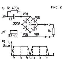
From the beginning of the positive half-cycle of the current through capacitor C1 to moment t1, the zener diode VD3 and diode VD2 are open, and the zener diode VD4 and diode VD1 are closed. In the time interval t1...t3, the zener diode VD3 and the diode VD2 remain open, and a stabilization current pulse passes through the opened zener diode VD4. The voltage at the output Uout and at the zener diode VD4 is equal to its stabilization voltage Ust.
The pulse stabilization current, which is through for a diode-zener diode rectifier, bypasses the RH load, which is connected to the bridge output. At time t2 the stabilization current reaches its maximum, and at time t3 it is zero. Until the end of the positive half-cycle, the zener diode VD3 and diode VD2 remain open.
At moment t4 the positive half-cycle ends and the negative half-cycle begins, from the beginning of which to moment t5 the zener diode VD4 and diode VD1 are already open, and the zener diode VD3 and diode VD2 are closed. In the time interval t5-t7, the zener diode VD4 and the diode VD1 continue to remain open, and a through stabilization current pulse passes through the zener diode VD3 at voltage UCT, the maximum at time t6. Starting from t7 and until the end of the negative half-cycle, the zener diode VD4 and diode VD1 remain open. The considered cycle of operation of the diode-zener diode rectifier is repeated in the following periods of mains voltage.
Thus, a rectified current passes through the zener diodes VD3, VD4 from the anode to the cathode, and a pulsed stabilization current passes in the opposite direction. In the time intervals t1...t3 and t5...t7, the stabilization voltage changes by no more than a few percent. The value of the alternating current at the input of the bridge VD1...VD4 is, to a first approximation, equal to the ratio of the network voltage to the capacitance of the ballast capacitor C1.
The operation of a diode-zener diode rectifier without a ballast capacitor, which limits the through current, is impossible. Functionally, they are inseparable and form a single whole - a capacitor-zener diode rectifier.
The spread in the UCT values of zener diodes of the same type is approximately 10%, which leads to additional ripples in the output voltage with the frequency of the supply network; the amplitude of the ripple voltage is proportional to the difference in the Ust values of zener diodes VD3 and VD4.
When using powerful zener diodes D815A...D817G, they can be installed on a common radiator if their type designation contains the letters "PP (zener diodes D815APP...D817GPP have reverse polarity of the terminals). Otherwise, the diodes and zener diodes must be swapped.
Transformerless power supplies are usually assembled according to the classical scheme: quenching capacitor, rectifier AC voltage, filter capacitor, stabilizer. A capacitive filter smoothes out output voltage ripples. The greater the capacitance of the filter capacitors, the less ripple and, accordingly, the greater the constant component of the output voltage. However, in some cases you can do without a filter, which is often the most cumbersome component of such a power source.
It is known that a capacitor connected to an alternating current circuit shifts its phase by 90°. A phase-shifting capacitor is used, for example, when connecting a three-phase motor to a single-phase network. If you use a phase-shifting capacitor in the rectifier, which ensures mutual overlap of half-waves of the rectified voltage, in many cases you can do without a bulky capacitive filter or significantly reduce its capacitance. The circuit of such a stabilized rectifier is shown in Fig. 3.
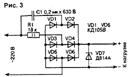
The three-phase rectifier VD1.VD6 is connected to an alternating voltage source through active (resistor R1) and capacitive (capacitor C1) resistances.
The output voltage of the rectifier stabilizes the zener diode VD7. Phase-shifting capacitor C1 must be designed for operation in alternating current circuits. Here, for example, capacitors of the K73-17 type with an operating voltage of at least 400 V are suitable.
Such a rectifier can be used where it is necessary to reduce the dimensions of an electronic device, since the dimensions of the oxide capacitors of a capacitive filter are, as a rule, much larger than those of a phase-shifting capacitor of a relatively small capacity.
Another advantage of the proposed option is that the current consumption is almost constant (in the case of a constant load), whereas in rectifiers with a capacitive filter, at the moment of switching on, the starting current significantly exceeds the steady-state value (due to the charge of the filter capacitors), which in some cases is extremely undesirable .
The described device can also be used with series voltage stabilizers that have a constant load, as well as with a load that does not require voltage stabilization.
A completely simple transformerless power supply (Fig. 4) can be built “on the knee” in literally half an hour.

In this embodiment, the circuit is designed for an output voltage of 6.8 V and a current of 300 mA. The voltage can be changed by replacing the zener diode VD4 and, if necessary, VD3. And by installing transistors on radiators, you can increase the load current. Diode bridge - any one designed for a reverse voltage of at least 400 V. By the way, you can also remember about the “ancient” diodes. D226B.
In another transformerless source (Fig. 5), the KR142EN8 microcircuit is used as a stabilizer. Its output voltage is 12 V. If adjustment of the output voltage is necessary, then pin 2 of the DA1 microcircuit is connected to the common wire through a variable resistor, for example, type SPO-1 (with a linear characteristic of resistance change). Then the output voltage can vary in the range of 12...22 V.
As a DA1 microcircuit, to obtain other output voltages, you need to use the appropriate integrated stabilizers, for example, KR142EN5, KR1212EN5, KR1157EN5A, etc. Capacitor C1 must have an operating voltage of at least 300 V, brand K76-3, K73-17 or similar (non-polar , high voltage). Oxide capacitor C2 acts as a power supply filter and smoothes out voltage ripples. Capacitor C3 reduces high frequency interference. Resistors R1, R2 are MLT-0.25 type. Diodes VD1...VD4 can be replaced with KD105B...KD105G, KD103A, B, KD202E. Zener diode VD5 with a stabilization voltage of 22...27 V protects the microcircuit from voltage surges when the source is turned on.

Despite the fact that theoretically capacitors in an AC circuit do not consume power, in reality they can generate some heat due to losses. You can check the suitability of a capacitor as a damping capacitor for use in a transformerless source by simply connecting it to the mains and assessing the temperature of the case after half an hour. If the capacitor manages to warm up noticeably, it is not suitable. Special capacitors for industrial electrical installations practically do not heat up (they are designed for large reactive power). Such capacitors are usually used in fluorescent lamps, in ballasts of asynchronous electric motors, etc.
In a 5-volt source (Fig. 6) with a load current of up to 0.3 A, a capacitor voltage divider is used. It consists of a paper capacitor C1 and two oxide capacitors C2 and C3, forming the lower (according to the circuit) non-polar arm with a capacity of 100 μF (counter-series connection of capacitors). The polarizing diodes for the oxide pair are bridge diodes. With the indicated ratings of the elements, the short circuit current at the output of the power supply is 600 mA, the voltage on capacitor C4 in the absence of load is 27 V.

The power supply unit for the portable receiver (Fig. 7) easily fits into its battery compartment. The diode bridge VD1 is designed for operating current, its maximum voltage is determined by the voltage provided by the zener diode VD2. Elements R3, VD2. VT1 form an analogue of a powerful zener diode. The maximum current and power dissipation of such a zener diode are determined by transistor VT1. It may require a heatsink. But in any case, the maximum current of this transistor should not be less than the load current. Elements R4, VD3 - circuit indicating the presence of output voltage. At low load currents, it is necessary to take into account the current consumed by this circuit. Resistor R5 loads the power circuit with a low current, which stabilizes its operation.

Quenching capacitors C1 and C2 are KBG type or similar. You can also use K73-17 with an operating voltage of 400 V (250 V is also suitable, since they are connected in series). The output voltage depends on the resistance of the quenching capacitors to alternating current, the actual load current and the stabilization voltage of the zener diode.
To stabilize the voltage of a transformerless power supply with a quenching capacitor, you can use symmetrical dinistors (Fig. 8).

When the filter capacitor C2 is charged to the opening voltage of the dinistor VS1, it turns on and bypasses the input of the diode bridge. The load at this time receives power from capacitor C2. At the beginning of the next half-cycle, C2 is again recharged to the same voltage, and the process is repeated. The initial discharge voltage of capacitor C2 does not depend on the load current and network voltage, therefore the stability of the unit’s output voltage is quite high.
The voltage drop across the dinistor when turned on is small, the power dissipation, and therefore its heating, is significantly less than that of a zener diode. The maximum current through the dinistor is about 60 mA. If this value is not enough to obtain the required output current, you can “power up the dinistor with a triac or thyristor (Fig. 9). The disadvantage of such power supplies is the limited choice of output voltages, determined by the switching voltages of the dinistors.

A transformerless power supply with adjustable output voltage is shown in Fig. 10a.
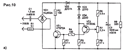
Its feature is the use of adjustable negative feedback from the output of the unit to the transistor stage VT1, connected in parallel with the output of the diode bridge. This stage is a regulatory element and is controlled by a signal from the output of a single-stage amplifier to VT2.
The output signal VT2 depends on the voltage difference supplied from the variable resistor R7, connected in parallel with the output of the power supply, and the reference voltage source on the diodes VD3, VD4. Essentially, the circuit is an adjustable parallel regulator. The role of the ballast resistor is played by the quenching capacitor C1, the parallel controlled element is played by the transistor VT1.
This power supply works as follows.
When connected to the network, transistors VT1 and VT2 are locked, and the storage capacitor C2 is charged through the diode VD2. When the base of transistor VT2 reaches a voltage equal to the reference voltage on diodes VD3, VD4, transistors VT2 and VT1 are unlocked. Transistor VT1 shunts the output of the diode bridge, and its output voltage drops, which leads to a decrease in the voltage on the storage capacitor C2 and to the blocking of transistors VT2 and VT1. This, in turn, causes an increase in voltage on C2, unlocking VT2, VT1 and repeating the cycle.
Due to the negative effect acting in this way feedback the output voltage remains constant (stabilized) both with the load on (R9) and without it (at idle). Its value depends on the position of the potentiometer R7.
The upper (according to the diagram) position of the engine corresponds to a higher output voltage. The maximum output power of the given device is 2 W. The output voltage adjustment limits are from 16 to 26 V, and with a short-circuited diode VD4 - from 15 to 19.5 V. The level of ripple on the load is no more than 70 mV.
Transistor VT1 operates in alternating mode: when there is a load - in linear mode, at idle - in pulse-width modulation (PWM) mode with a voltage pulsation frequency on capacitor C2 of 100 Hz. In this case, the voltage pulses on the VT1 collector have flat edges.
The criterion for the correct choice of capacitance C1 is to obtain the required maximum voltage at the load. If its capacity is reduced, then the maximum output voltage at the rated load is not achieved. Another criterion for choosing C1 is the constancy of the voltage oscillogram at the output of the diode bridge (Fig. 10b).

The voltage oscillogram has the form of a sequence of rectified sinusoidal half-waves of the mains voltage with limited (flattened) peaks of positive half-sine waves; the amplitude of the peaks is a variable value, depending on the position of the R7 slider, and changes linearly as it rotates. But each half-wave must necessarily reach zero; the presence of a constant component (as shown in Fig. 10b by the dotted line) is not allowed, because in this case, the stabilization regime is violated.
The linear mode is lightweight, transistor VT1 heats up little and can operate practically without a heatsink. Slight heating occurs in the lower position of the R7 engine (at minimum output voltage). At idle, the thermal regime of transistor VT1 worsens in the upper position of the R7 engine. In this case, transistor VT1 should be installed on a small radiator, for example, in the form of a “flag” made of a square aluminum plate with a side of 30 mm and a thickness of 1...2 mm.
Regulating transistor VT1 is of medium power, with a high transmission coefficient. His collector current must be 2...3 times greater than the maximum load current, the permissible collector-emitter voltage is not less than the maximum output voltage of the power supply. Transistors KT972A, KT829A, KT827A, etc. can be used as VT1. Transistor VT2 operates in low current mode, so any low-power pnp transistor is suitable - KT203, KT361, etc.
Resistors R1, R2 are protective. They protect the control transistor VT1 from failure due to current overload during transient processes when the unit is connected to the network.
The transformerless capacitor rectifier (Fig. 11) operates with auto-stabilization of the output voltage. This is achieved by changing the connection time of the diode bridge to the storage capacitor. Transistor VT1, operating in switch mode, is connected parallel to the output of the diode bridge. The VT1 base is connected through a zener diode VD3 to a storage capacitor C2, separated by direct current from the bridge output by a diode VD2 to prevent rapid discharge when VT1 is open. As long as the voltage at C2 is less than the stabilization voltage VD3, the rectifier operates as usual. When the voltage on C2 increases and VD3 opens, transistor VT1 also opens and shunts the output of the rectifier bridge. The voltage at the bridge output decreases abruptly to almost zero, which leads to a decrease in the voltage at C2 and the zener diode and the key transistor are turned off.

Next, the voltage on capacitor C2 increases again until the zener diode and transistor are turned on, etc. The process of auto-stabilization of the output voltage is very similar to the operation pulse stabilizer voltage with pulse-width regulation. Only in the proposed device the pulse repetition rate is equal to the voltage ripple frequency at C2. To reduce losses, the key transistor VT1 must have a high gain, for example, KT972A, KT829A, KT827A, etc. You can increase the output voltage of the rectifier by using a higher-voltage zener diode (a chain of low-voltage ones connected in series). With two zener diodes D814V, D814D and a capacitance of capacitor C1 of 2 μF, the output voltage across a load with a resistance of 250 Ohms can be 23...24 V.
Similarly, you can stabilize the output voltage of a half-wave diode-capacitor rectifier (Fig. 12).
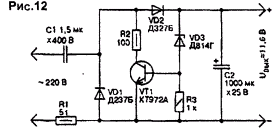
For a rectifier with a positive output voltage, an n-p-n transistor is connected in parallel with the diode VD1, controlled from the output of the rectifier through a zener diode VD3. When capacitor C2 reaches a voltage corresponding to the moment the zener diode opens, transistor VT1 also opens. As a result, the amplitude of the positive half-wave voltage supplied to C2 through the diode VD2 is reduced to almost zero. When the voltage on C2 decreases, transistor VT1 closes thanks to the zener diode, which leads to an increase in the output voltage. The process is accompanied by pulse-width regulation of the pulse duration at input VD2, therefore, the voltage on capacitor C2 is stabilized.
In a rectifier with a negative output voltage, a pnp transistor KT973A or KT825A must be connected in parallel with the diode VD1. The output stabilized voltage on a load with a resistance of 470 Ohms is about 11 V, the ripple voltage is 0.3...0.4 V.
In both options, the zener diode operates in a pulsed mode at a current of a few milliamps, which is in no way related to the rectifier load current, the variation in the capacitance of the quenching capacitor and fluctuations in the network voltage. Therefore, losses in it are significantly reduced, and it does not require a heat sink. The key transistor also does not require a radiator.
Resistors R1, R2 in these circuits limit the input current during transient processes at the moment the device is connected to the network. Due to the inevitable “bouncing” of the contacts of the power plug, the switching process is accompanied by a series of short-term short circuits and open circuits. During one of these short circuits, the quenching capacitor C1 can be charged to the full amplitude value of the network voltage, i.e. up to approximately 300 V. After a break and subsequent closure of the circuit due to “bounce”, this and mains voltage can add up to a total of about 600 V. This is the worst case and must be taken into account to ensure reliable operation of the device.
Another version of the key transformerless power supply circuit is shown in Fig. 13.

The mains voltage, passing through the diode bridge on VD1.VD4, is converted into a pulsating amplitude of about 300 V. Transistor VT1 is a comparator, VT2 is a switch. Resistors R1, R2 form a voltage divider for VT1. By adjusting R2 you can set the response voltage of the comparator. Until the voltage at the output of the diode bridge reaches the set threshold, the transistor VT1 is closed, the gate VT2 has an unlocking voltage and is open. Capacitor C1 is charged through VT2 and diode VD5.
When the set operating threshold is reached, transistor VT1 opens and bypasses the gate VT2. The key closes and will open again when the voltage at the bridge output becomes less than the comparator operating threshold. Thus, a voltage is established on C1, which stabilizes integral stabilizer DA1.
With the ratings shown in the diagram, the source provides an output voltage of 5 V at a current of up to 100 mA. The setting consists of setting the response threshold VT1. You can use IRF730 instead. KP752A, IRF720, BUZ60, 2N6517 is replaced by KT504A.
A miniature transformerless power supply for low-power devices can be built on the HV-2405E chip (Fig. 14), which directly converts alternating voltage to direct voltage.

The input voltage range of the IC is -15...275 V. The output voltage range is 5...24 V with a maximum output current of up to 50 mA. Available in a flat plastic housing DIP-8. The structure of the microcircuit is shown in Fig. 15a, the pinout is shown in Fig. 15b.


In the source circuit (Fig. 14), special attention should be paid to resistors R1 and R2. Their total resistance should be around 150 Ohms, and the dissipated power should be at least 3 W. The input high-voltage capacitor C1 can have a capacitance from 0.033 to 0.1 μF. Varistor Rv can be used in almost any type with an operating voltage of 230.250 V. Resistor R3 is selected depending on the required output voltage. In its absence (outputs 5 and 6 are closed), the output voltage is slightly more than 5 V; with a resistance of 20 kOhm, the output voltage is about 23 V. Instead of a resistor, you can turn on a zener diode with the required stabilization voltage (from 5 to 21 V). There are no special requirements for other parts, with the exception of the choice of operating voltage of electrolytic capacitors (calculation formulas are shown in the diagram).
Considering the potential danger of transformerless sources, in some cases a compromise option may be of interest: with a quenching capacitor and a transformer (Fig. 16).

A transformer with a high-voltage secondary winding is suitable here, since the required rectified voltage is set by selecting the capacitance of capacitor C1. The main thing is that the transformer windings provide the required current.
To prevent the device from malfunctioning when the load is disconnected, a D815P zener diode should be connected to the output of the VD1...VD4 bridge. In normal mode, it does not work, since its stabilization voltage is higher than the operating voltage at the bridge output. Fuse FU1 protects the transformer and stabilizer in case of breakdown of capacitor C1.
In sources of this type, voltage resonance may occur in a circuit of series-connected capacitive (capacitor C1) and inductive (transformer T1) resistances. This should be remembered when setting them up and monitoring the voltages with an oscilloscope.
See other articles section.

