29.06.2020
Power supply circuit 5 volt 2 ampere. Simple power supply. Features of pulse stabilizers
Somehow recently I came across a circuit on the Internet for a very simple power supply with the ability to adjust the voltage. The voltage could be adjusted from 1 Volt to 36 Volt, depending on the output voltage on the secondary winding of the transformer.
Take a close look at the LM317T in the circuit itself! The third leg (3) of the microcircuit is connected to capacitor C1, that is, the third leg is INPUT, and the second leg (2) is connected to capacitor C2 and a 200 Ohm resistor and is an OUTPUT.
Using a transformer from mains voltage 220 Volts we get 25 Volts, no more. Less is possible, no more. Then we straighten the whole thing with a diode bridge and smooth out the ripples using capacitor C1. All this is described in detail in the article on how to obtain constant voltage from alternating voltage. And here is our most important trump card in the power supply - this is a highly stable voltage regulator chip LM317T. At the time of writing, the price of this chip was around 14 rubles. Even cheaper than a loaf white bread.
Description of the chip
LM317T is a voltage regulator. If the transformer produces up to 27-28 volts on the secondary winding, then we can easily regulate the voltage from 1.2 to 37 volts, but I would not raise the bar to more than 25 volts at the transformer output.
The microcircuit can be executed in the TO-220 package:

or in D2 Pack housing

It can pass a maximum current of 1.5 Amps, which is enough to power your electronic gadgets without voltage drop. That is, we can output a voltage of 36 Volts with a current load of up to 1.5 Amps, and at the same time our microcircuit will still output 36 Volts - this, of course, is ideal. In reality, fractions of volts will drop, which is not very critical. With a large current in the load, it is more advisable to install this microcircuit on a radiator.
In order to assemble the circuit, we also need a variable resistor of 6.8 Kilo-Ohms, or even 10 Kilo-Ohms, as well as a constant resistor of 200 Ohms, preferably from 1 Watt. Well, we put a 100 µF capacitor at the output. Absolutely simple scheme!
Assembly in hardware
Previously, I had a very bad power supply with transistors. I thought, why not remake it? Here is the result ;-)

Here we see the imported GBU606 diode bridge. It is designed for a current of up to 6 Amps, which is more than enough for our power supply, since it will deliver a maximum of 1.5 Amps to the load. I installed the LM on the radiator using KPT-8 paste to improve heat transfer. Well, everything else, I think, is familiar to you.
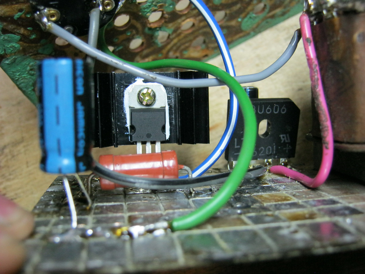
And here is an antediluvian transformer that gives me a voltage of 12 volts on the secondary winding.

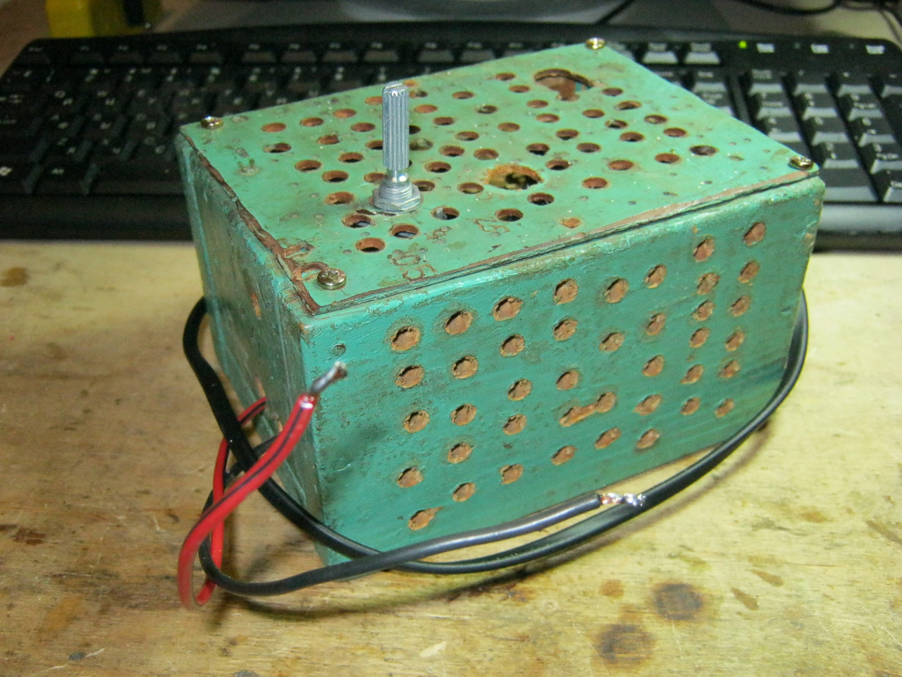
We carefully pack all this into the case and remove the wires.

So what do you think? ;-)
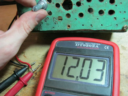
The minimum voltage I got was 1.25 Volts, and the maximum was 15 Volts.

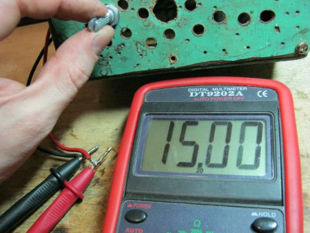
I set any voltage, in this case the most common are 12 Volts and 5 Volts

Everything works great!
This power supply is very convenient for adjusting the speed of a mini drill, which is used for drilling circuit boards.

Analogues on Aliexpress
By the way, on Ali you can immediately find a ready-made set of this block without a transformer.

Too lazy to collect? You can buy a ready-made 5 Amp for less than $2:

You can view it at this link.
If 5 Amps is not enough, then you can look at 8 Amps. It will be enough for even the most seasoned electronics engineer:

5 volts is one of the most widely used voltages. Most programmable and non-programmable microcontrollers, all kinds of indicators and testers are powered from this voltage. In addition, 5 volts is used to charge all kinds of gadgets: phones, tablets, players, and so on. I'm sure every radio amateur can come up with many uses for this voltage. And in this regard, I have prepared for you three good, in my opinion, options for power supplies with a stabilized output voltage of 5 volts.
The first option is the simplest.
This option is distinguished by a minimal number of parts used, extreme ease of assembly and incredible ‘survivability’ - the block is almost impossible to kill. So let's move on to the diagram.
This circuit is copied from an inexpensive phone charger, has output voltage stabilization and is capable of delivering a current of up to 0.5 A. In fact, the unit can output more, but when the current at the output increases, overload protection begins to operate and output voltage begins to decrease. Protection against overloads and short circuits is implemented on a 10 ohm resistor in the emitter circuit of the power transistor and a low-power transistor s9014. When the current through the primary winding of the transformer increases, a voltage drop is created on the emitter resistor sufficient to open s9014, which in turn pulls the base of the power transistor to negative, thereby closing it and reducing the duration of the pulses through the primary winding. By changing the value of this resistor, you can increase or decrease the protection operation current. You should not increase it too much, as this will entail an increase in heating of the power transistor and increase the likelihood of the latter failing.
Stabilization is performed using a common optocoupler pc817 and on the zener diode 3.9 V (by changing the value of which you can change the output voltage). When the output voltage is exceeded, the optocoupler LED begins to glow brighter, causing an increase in the current through the optocoupler transistor to the s9014 base and, as a result, closing the power switch. When the output voltage decreases, on the contrary, the optocoupler transistor will begin to close and s9014 will not interrupt the pulses based on the power switch, thereby increasing their duration and, accordingly, increasing the output voltage.
Particular attention should be paid to winding the transformer. This is often a factor that pushes beginners away from switching power supplies. So, since the block is single-ended, we will need a transformer with a non-magnetic gap between the core halves. The gap is needed to quickly demagnetize the core and to prevent the ferrite from entering saturation. Transformer calculations should ideally be carried out in special programs, but for those who don’t want to do this, I’ll say that in such low-power power supplies, the primary winding consists of 190-220 turns of 0.08-0.1mm wire. Roughly speaking, the larger the core, the fewer turns. The base winding is wound on top of the primary in the same direction. It consists of 7 - 15 turns of the same wire. And at the end the secondary is wound with a thicker wire. The number of turns is 5-7. It is extremely important to wind all the windings in the same direction and remember where the beginning and end are. On the diagram and on the board (which you can download here), the dots indicate the beginning of the windings.
There is nothing more to add regarding the scheme; it is quite simple and does not require any special skills for assembly. All components can be changed within 25%, the unit will work perfectly. The power transistor can be installed with any reverse conductivity corresponding to the power and with a calculated collector voltage of at least 400 volts. The base transistor is any low-power NPN with the same pinout as s9014.
This unit can be powerfully used where high current is not needed, but compactness is needed, for example, for powering Arduino or for charging devices with small-capacity batteries. The advantages of this power supply include its compactness, the presence of protection and stabilization, and, of course, ease of assembly. The only downside is, perhaps, the low output power, which, by the way, can be increased by increasing the capacity of the input filter capacitor.
By the way, the block looks like this:
The second option is more powerful.
This option is very similar to the previous one, but more powerful. The block has a modified feedback and therefore better stabilization. Let's take a look at the diagram.
The circuit is a standby power supply unit for a computer power supply. Unlike the previous circuit, this one has a more powerful power transistor, a larger input filter capacitor and, most importantly, a transformer with a larger overall power. All this just affects output power. Also in this circuit, unlike the first, normal stabilization is done on the TL431 - the reference voltage source.
The principle of operation here is the same as the previous option. An initial bias voltage is applied through a 560 kOhm resistor to the base of the power switch, it opens slightly and current begins to flow through the primary winding. An increase in current in the primary causes an increase in current in all other windings, which means that the current arising in the base winding will open the transistor even more, and this process will continue until the transistor is completely open. When it opens, the current through the primary will stop changing, which means the secondary will stop flowing and the transistor will close and the cycle will repeat.
I spoke in detail about the operation of current protection and stabilization above and see no point in repeating myself, since everything works exactly the same here.
Since this power supply is made on the basis of a computer unit, I used a ready-made transformer and did not rewind it. Transformer EEL-19B. Estimated overall power 15 – 20 W.
As in the previous circuit, the component values can be deviated within 25%, since in different computer power supplies this circuit works perfectly with different components. This instance, thanks to the output current of 2 A, can be used as a charger for phones and tablets or for other consumers requiring high current. One of the advantages of this design is the ease of obtaining radio components, because everyone probably has a non-working power supply from an old computer or TV, and there the elementary base is enough for 3 - 4 such power supplies. Also a plus can be considered a considerable output current and good stabilization. Of the minuses, we can rightly note the size of the board (it is quite high due to the transformer) and the possibility of whistling during idle. The whistle may appear due to a malfunction of some element, or simply due to the conversion frequency being too low at idle. Under load the frequency increases.
The third option is the most powerful.
This option is for those who need enormous power and excellent stabilization. If you don't mind sacrificing compactness, this unit is especially for you. So, let's look at the diagram.
Unlike the previous two options, this one uses a specialized PWM controller UC3843, which, unlike transistors, can somehow change the pulse width and is specially made for use in single-cycle power supplies. Also, with UC, the frequency does not change depending on the load and it can be clearly calculated in specialized calculators.
So the principle of operation. The initial power is supplied through a 300 kOhm resistor to the 7th leg of the microcircuit, it starts up and begins to generate pulses that come out from the 6th leg and go to the field device. The frequency of these same pulses depends on the elements Rt and Ct. With the specified components, the output frequency is 78.876 kHz. By the way, here is the device of the microcircuit:
This microcircuit is very convenient to implement current protection; it has a special output for this – current sense. If the voltage is more than 1 volt, the protection will work on this leg and the controller will reduce the duration of the pulses. Stabilization here is done using the built-in error amplifier current sense comparator. Since we have 0 volts at pin 2, the amplifier is error amp. It always produces a logical one and it goes to the input of the current sense comparator amplifier, thereby forming a reference voltage of 1 volt at its inverting input. When the voltage at the output of the power supply exceeds, the phototransistor of the optocoupler opens and shunts 1 pin of the microcircuit to minus. In this case, the voltage at the inverting input of the current sense comparator decreases, and since the voltage at its non-inverting transistor at the moment of opening increases, at some point it will exceed the voltage at the inverting input (the same thing happens during a short circuit) and the current sense comparator will produce a logical unit, which in turn will lead to a decrease in the pulse duration and, ultimately, to a decrease in the voltage at the output of the power supply. The stabilization in this power supply is very good, so that you understand how good it is, when you connect a 1 Ohm resistor to the output, the voltage drops by only 0.06 volts, while 25 W of heat is dissipated on it and it burns out in a couple of seconds. In general, this unit can output both 30 W and 35, since it is used here as a key field-effect transistor. The diagram shows 4n60, but I used irf840 since I have a lot of them. The microcircuit can supply a current of up to 1 A to control the field switch, which makes it possible to control fairly powerful field switches without an additional driver.
The at 5 volts can be used to power a low-power load, for example, an electronic thermometer, a microcalculator, an electronic watch.
Technical parameters of a switching power supply
- Input voltage - 220 ±15% V;
- Conversion frequency - 35 kHz;
- Maximum load power - 3 W;
- Efficiency - up to 75%;
The basic module of this switching power supply is a voltage converter on transformer T1 and transistors VT1, VT2, built using a half-bridge circuit. Diode bridge rectifies AC voltage networks. A parametric stabilizer is built on radioelements R1, VD2 - VD4, which, together with capacitors C2 - C4, creates a voltage divider.
To power the master oscillator, the voltage removed from VD2 is used. Resistance R1 plays a dual role: on the one hand, it acts as a ballast in the stabilizer, thereby forming a voltage boost for capacitance C8, and on the other hand, it reduces the current consumption from the mains at the moment of an accidental short circuit at the output of a switching power supply.
Operational amplifier DD1 connected according to a multivibrator circuit forms a master oscillator. Capacitance C7 provides galvanic isolation between the master oscillator and VT2.
Transformer T1 is assembled on a ferrite ring of grade 2000NM and size K12x8x3. Its windings contain: I – 500 vit. enameled wire PEV-2 with a diameter of 0.15 mm, II - 50 vit. (for 5 volts) of the same wire with a diameter of 0.31 with a tap in the middle.
Setting up a switching power supply consists of selecting resistances R1 and R9 for a certain load current value. Resistance R9 is selected based on the need to saturate transistor VT1, which is determined using an oscilloscope.
The value of R1 must be selected such that, under normal load, the current flowing through the zener diodes VD3 and VD4 is more than 5 mA. To reduce voltage ripple at the output, the values of capacitances C3, C4 must be doubled. In addition, it is still possible to reduce the magnitude of the ripple by adding a 50...100 µF oxide capacitor in parallel with capacitance C6 for a rated voltage of 10 V.
Everyone knows that there is such an operation as pre-sale preparation of goods. A simple but very necessary action. By analogy with it, I have long been using pre-use preparation of all purchased Chinese-made goods. There is always the possibility of modification in these products, and I note that it is really necessary, which is a consequence of the manufacturer saving on high-quality material for its individual elements or not installing them at all. Let me be suspicious and suggest that all this is not accidental, but is an integral element of the manufacturer’s policy aimed ultimately at reducing the service life of the manufactured product, which results in an increase in sales. Having decided to actively use a miniature electric massager (of course, made in China), I immediately drew attention to its power supply, which looks similar to Charger mobile phone and even with the inscription COURIER CHARGER- mobile charger. Having an OUTPUT of 5 volts and 500 mA. Without even being convinced of its serviceability, I took it apart and looked at the contents.
The electronic components installed on the board and especially the zener diode at the output indicated that this was indeed a power supply. By the way, I don’t consider the absence of a diode bridge to be a positive thing.

The connected load, in the form of two 2.5 V light bulbs in series, with a current consumption of 150 mA, detected 5.76 V at the output. The device is designed to be powered by three AA batteries - 4.5 V, I think acceptable, and 5 V from the adapter, but anything else, in this particular case, is clearly useless.

After searching for a schematic on the Internet, I chose to draw, based on a photo taken in advance, a printed circuit board with the electronic components located on it.
Adapter circuit and conversion

Image printed circuit board made it possible to draw the existing power supply diagram. The CHY 1711 transistor optocoupler, C945, S13001 transistors and other components did not allow me to call the circuit primitive, but with the existing ratings of some components and the absence of others, it did not suit me.

IN new scheme a 160 mA fuse was introduced, and instead of the existing rectifier, a diode bridge consisting of 4 1N4007 diodes was introduced. The value of the zener diode VD3 controlling the optocoupler has been changed from 4V6 to 3V6, which should reduce the output voltage to the desired level.

There was enough free space on the board so that it was not difficult to implement the planned changes. The newly assembled power supply had an output voltage of almost 4.5 volts.

And current output up to 300 mA inclusive.

As a result, a number of additional electronic components and time spent interesting work, gave me the opportunity to have a decent power supply, which I hope will serve faithfully for a long time. Babay was involved in debugging the power supply.

