29.06.2020
bipolar transistors. Deciphering the symbols on the multimeter. What do the buttons and icons mean? hfe gain
The bipolar transistor is one of the oldest, but the most well-known type of transistor, and is still used in modern electronics. The transistor is indispensable when it is necessary to drive a sufficiently powerful load for which the control device cannot provide sufficient current. They are different type and power, depending on the tasks performed. You can find basic knowledge and formulas about transistors in this article.
Introduction
Before starting the lesson, let's agree that we are discussing only one type of way to turn on a transistor. A transistor can be used in an amplifier or a receiver, and generally each transistor model is produced with certain characteristics to make it more highly specialized for better work in a certain setting.
The transistor has 3 terminals: base, collector and emitter. It is impossible to say unequivocally which of them is the input and which is the output, since they are all connected and affect each other in one way or another. When the transistor is turned on in switch mode (load control), it acts like this: the base current controls the current from the collector to the emitter or vice versa, depending on the type of transistor.
There are two main types of transistors: NPN and PNP. To understand this, we can say that the main difference between these two types is the direction of the electric current. This can be seen in figure 1.A, where the direction of the current is indicated. In an NPN transistor, one current flows from the base into the transistor and another current flows from the collector to the emitter, while in a PNP transistor it is the other way around. From a functional point of view, the difference between these two types of transistors is the load voltage. As you can see in the picture, the NPN transistor provides 0V when it is on, while the PNP provides 12V. You will see later why this affects the choice of transistor.
For simplicity, we will only study NPN transistors, but all this applies to PNP, taking into account that all currents are reversed.
The figure below shows the analogy between a switch (S1) and a transistor switch, where you can see that the base current closes or opens the path for current from the collector to the emitter:
Knowing exactly the characteristics of the transistor, you can get the most out of it. The main parameter is the DC gain of the transistor, which is usually denoted H fe or β. It is also important to know the maximum current, power and voltage of the transistor. These parameters can be found in the documentation for the transistor, and they will help us determine the value of the resistor on the base, which is described next.
Using an NPN transistor as a switch
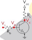
The figure shows the inclusion of an NPN transistor as a switch. You will meet this inclusion very often when analyzing various electronic circuits. We will study how to run the transistor in the selected mode, calculate the base resistor, current gain of the transistor and load resistance. I suggest the simplest and most accurate way to do this.
1. Assume the transistor is in saturation mode: Wherein mathematical model transistor becomes very simple, and we know the voltage at the point V c . We will find the value of the base resistor at which everything will be correct.
2. Determination of collector saturation current: The voltage between the collector and the emitter (V ce) is taken from the documentation of the transistor. The emitter is connected to GND, respectively V ce = V c - 0 = V c . Once we know this value, we can calculate the collector saturation current using the formula:
Sometimes, the load resistance R L is unknown or cannot be accurate, like the resistance of a relay winding; In this case, it is enough to know the current required to start the relay.
Make sure the load current does not exceed the maximum collector current of the transistor.
3. Calculation of the required base current: Knowing the collector current, one can calculate the minimum required base current to achieve this collector current using the following formula:
From it follows that:
4. Exceeding the allowable values: After you have calculated the base current, and if it turned out to be lower than that specified in the documentation, then you can overload the transistor by multiplying the calculated base current, for example, by 10 times. Thus, the transistor switch will be much more stable. In other words, the performance of the transistor will decrease if the load is increased. Be careful, try not to exceed the maximum base current specified in the documentation.
5. Calculation of the required value of R b: Considering an overload of 10 times, the resistance R b can be calculated using the following formula:
where V 1 is the transistor control voltage (see fig 2.a)
But if the emitter is connected to ground and the base-emitter voltage is known (about 0.7V for most transistors), and assuming V 1 = 5V, the formula can be simplified to the following: ![]()
It can be seen that the base current is multiplied by 10, taking into account the overload.
When the value of R b is known, the transistor is "set" to act as a switch, also called "saturation and cutoff mode", where "saturation" is when the transistor is fully open and conducts current, and "cut off" is when it is closed and no current is conducting. .
Note: When we say , we are not saying that the collector current should be . It simply means that the collector current of the transistor can rise to that level. The current will follow Ohm's laws, like any electricity.
Load calculation
When we considered that the transistor is in saturation mode, we assumed that some of its parameters did not change. This is not entirely true. In fact, these parameters were changed mainly by increasing the collector current, and therefore it is safer for overload. The documentation indicates a change in the parameters of the transistor during overload. For example, the table in Figure 2.B shows two parameters that change significantly:
H FE (β) varies with collector current and voltage V CEsat . But VCEsat itself varies with collector and base current as shown in the table below.

The calculation can be very complicated, since all the parameters are closely and intricately interconnected, so it is better to take the worst values. Those. the smallest is H FE , the largest is V CEsat and V CEsat .
Typical transistor switch application

In modern electronics, a transistor switch is used to control electromagnetic relays that consume up to 200 mA. If you want to control a relay with a logic chip or microcontroller, then the transistor is indispensable. In figure 3.A, the resistance of the base resistor is calculated depending on the current required for the relay. Diode D1 protects the transistor from the pulses that the coil generates when turned off.
2. Open collector transistor connection:

Many devices, such as the 8051 microcontroller family, have open collector ports. The resistance of the base resistor of the external transistor is calculated as described in this article. Note that the ports can be more complex and often use FETs instead of bipolars and are called open-drain outputs, but everything remains exactly the same as in Figure 3.B
3. Creation of a logical element OR-NOT (NOR):

Sometimes a circuit needs to use a single gate and you don't want to use a 14-pin IC with 4 gates, either because of cost or board space. It can be replaced by a pair of transistors. Note that the frequency response of such elements depends on the characteristics and type of transistors, but usually below 100 kHz. Reducing the output resistance (Ro) will increase the power consumption but increase the output current.
You need to find a compromise between these parameters.
The figure above shows a NOR gate built using 2x 2N2222 transistors. This can be done with PNP 2N2907 transistors, with minor modifications. You just have to consider that all electrical currents then flow in the opposite direction.
Finding errors in transistor circuits
When a problem occurs in circuits containing many transistors, it can be quite difficult to know which one is bad, especially when they are all soldered. I give you some tips that will help you find the problem in such a circuit fairly quickly:
1.Temperature: If the transistor gets very hot, there is probably a problem somewhere. Not necessarily that the problem is in the hot transistor. Usually a defective transistor does not even heat up. This rise in temperature may be caused by another transistor connected to it.
2. Measurement of V CE transistors: If they are all the same type and all work, then they should have approximately the same VCE. Finding transistors having different V CE is fast way detection of defective transistors.
3. Measuring the voltage across the base resistor: The voltage across the base resistor is quite important (if the transistor is on). For a 5V NPN transistor driver, the voltage drop across the resistor should be more than 3V. If there is no voltage drop across the resistor, then either the transistor or the transistor driver is defective. In both cases, the base current is 0.
h FE of a transistor is the current gain or amplification factor of a transistor.
h FE (which is also referred to as β) is the factor by which the base current is amplified to produce the amplified current of the transistor. The unamplified current is the base current, which then undergoes amplification by a factor of h FE to produce an amplified current which flows through the collector and emitter terminals.
A transistor works by feeding a current into the base of the transistor. The base current is then amplified by h FE to yield its amplified current. The formula is below:
I C = hFE I B =βI B
So if 1mA is fed into the base of a transistor and it has a h FE of 100, the collector current will be 100mA.
Every transistor has its own unique h FE . The h FE is normally seen to be a constant value, normally around 10 to 500, but it may change slightly with temperature and with changes in collector-to-emitter voltage.
Check the transistor"s datasheet for the h FE value in its specifications.
Note that h FE may refer to DC or AC current gain. Many datasheets may just specify one value, such as the DC gain. The datasheets will normally specify whether the h FE value is for DC or AC current gain.
Also, note that as the h FE value is highly variable, many datasheets will specify a minimum and maximum h FE for the transistor. It is very hard for transistors to be produced with a precise h FE value during the manufacturing process. Therefore, manufacturers generally specify a range that h FE may be within.
Because h FE is so widely variable and unpredictable in nature, good transistor circuit design is important to give stable, predictable amplification for transistor circuits to account for this unpredictability.
So, let's agree in advance that in our examples we will use a circuit with a OE (Common Emitter):
The advantages of this circuit are such that this circuit amplifies both voltage and current. Therefore, this circuit is most often used in electronics.
Well, let's start studying the amplifying properties of the transistor with this circuit. This scheme has very interesting parameter. It is called the current gain in the Common Emitter circuit and is denoted by the letter β
(beta). This coefficient shows how many times the collector current exceeds the base current in the active mode of the transistor

Also often, especially on multimeters, it is denoted as h21e or hfe.
Finding beta in practice
Let's put together a schematic, with the help of which, I think, everything will fall into place. Using this scheme, we will approximately measure the coefficient β .
For an NPN transistor, the circuit would look like this:

For a PNP transistor like this:


Since its conductivity is NPN, therefore, we will use this scheme:
So what do we see here? There is a transistor, two power supplies and two ammeters. We set one ammeter to measure microamps (µA), and the second to measure milliamps (mA). On the power supply Bat 2 set the voltage to 9 volts. power unit Bat 1 we have an arrow. So we will change its value from 0 to 1 Volt.
We have a scheme with OE. Through the base-emitter and further along the circuit, we have a base current flowing I B, and through the collector-emitter and further along the circuit, the collector current is carried I K. In order to measure this current (current strength), we hooked an ammeter into the circuit break. It remains a small matter. Measure base current (I B), measure the collector current (I K) and then stupidly divide the collector current by the base current. And from this ratio we will approximately find the coefficient β . Everything is simple).
Here are two power supplies:

Exhibit on Bat 2 voltage at 9 volts:

The whole scheme looks like this

The yellow multimeter will measure milliamps, and the red one will measure microamps, so we don’t pay attention to the comma on the red multimeter.
Add voltage to Bat 1 from 0.6 Volt and turn the knob up to 1 Volt, not forgetting to photograph the results. We calculate the coefficient β for some measurements:

24.6mA/0.23mA=107

50.6mA/0.4mA=126.5

53.4mA/0.44mA=121.4

91.1mA/0.684mA=133.2

99.3mA/0.72mA=137.9

124.6mA/0.827mA=150.6

173.3mA/1.095mA=158
Finding the arithmetic mean:
β≈(107+126.5+121.4+133.2+137.9+150.6+158)/7=133
In the datasheet on KT815B, the coefficient β
can have a value in the range from 50 to 350. Our coefficient fits well into this range, which means the transistor is alive and well. Will intensify.
I want to add that the true value of the coefficient β measured a little differently. To determine the true value, it is necessary to measure not direct currents, as we did, but very small increments of these currents, that is, to measure on alternating current and a small signal:
.png)
With a small direct current, the measured value of the beta coefficient is less than the real one, and with a large direct current, it is greater than the real one. The truth is somewhere in the middle. Radio amateurs are not picky people and in the field the main thing is to approximately find out the value β .
I also really liked the video about the bipolar transistor from Soldering TV. I recommend to watch without fail:
A transistor is a semiconductor device, the main purpose of which is to be used in circuits for amplifying or generating signals, as well as for electronic keys.
Unlike a diode, a transistor has two p-n junctions connected in series. Between the transitions there are zones with different conductivity (type "n" or type "p"), to which the terminals are connected for connection. The output from the middle zone is called the "base", and from the extreme - "collector" and "emitter".
The difference between the "n" and "p" zones is that the first has free electrons, while the second has the so-called "holes". Physically, "hole" means the lack of an electron in the crystal. Electrons under the action of the field created by the voltage source move from minus to plus, and "holes" - vice versa. When regions with different conductivity are connected to each other, electrons and “holes” diffuse and an area called a p-n junction is formed at the connection boundary. Due to diffusion, the “n” region turns out to be positively charged, and “p” negatively, and between regions with different conductivity, an own electric field arises, concentrated in the region of the p-n junction.
When the positive output of the source is connected to the “p” area, and the minus to the “n” area, its electric field compensates for the p-n junction's own field, and an electric current passes through it. When connected back, the field from the power source is added to its own, increasing it. The junction is locked, and current does not pass through it.

The transistor has two junctions: collector and emitter. If you connect the power supply only between the collector and the emitter, then no current will flow through it. One of the passages is blocked. To open it, potential is supplied to the base. As a result, a current arises in the collector-emitter section, which is hundreds of times greater than the base current. If the base current changes with time, then the emitter current exactly repeats it, but with a larger amplitude. This is the reason for the amplifying properties.
Depending on the combination of alternation of conduction bands, transistors are p-n-p or n-p-n. PNP transistors open with a positive potential at the base, and n-p-n - with a negative one.
![]()
Consider several ways to test a transistor with a multimeter.
Checking the transistor with an ohmmeter
Since the transistor has two p-n junctions, their serviceability can be checked by the method used to test semiconductor diodes. To do this, it can be represented as the equivalent of a back-to-back connection of two semiconductor diodes.

The eligibility criteria for them are:
- Low (hundreds of ohms) resistance when connecting the source direct current in the forward direction;
- Infinitely high resistance when connected to a DC source in the opposite direction.
A multimeter or tester measures resistance using its own auxiliary power source - a battery. Its voltage is small, but it is enough to open the p-n junction. By changing the polarity of connecting the probes from the multimeter to a working semiconductor diode, in one position we get a resistance of a hundred ohms, and in the other - infinitely large.
A semiconductor diode is rejected if
- in both directions, the device will show a break or zero;
- in the opposite direction, the device will show any significant resistance value, but not infinity;
- instrument readings will be unstable.
When testing a transistor, six resistance measurements with a multimeter will be required:
- base-emitter direct;
- base-collector direct;
- base-emitter reversed;
- base-collector reverse;
- emitter-collector direct;
- emitter-collector reverse.
The serviceability criterion when measuring the resistance of the collector-emitter section is a break (infinity) in both directions.
Transistor Gain
There are three schemes for connecting a transistor to amplifying stages:
- with a common emitter;
- with a common collector;
- with a common base.
All of them have their own characteristics, and the most common scheme is with a common emitter. Any transistor is characterized by a parameter that determines its amplifying properties - the gain. It shows how many times the current at the output of the circuit will be greater than at the input. Each of the switching circuits has its own coefficient, which is different for the same element.
The reference books give the coefficient h21e - the gain for a circuit with a common emitter.
How to Test a Transistor by Measuring Gain
One of the methods for checking the health of a transistor is to measure its gain h21e and compare it with the passport data. The handbooks give the range in which the measured value can be for of this type semiconductor device. If the measured value is within the range, then it is OK.
The gain measurement is also carried out for the selection of components with the same parameters. This is necessary to build some amplifier and oscillator circuits.
To measure the h21e coefficient, the multimeter has a special measurement limit, designated hFE. The letter F stands for "forward" (straight polarity), and "E" for a common emitter circuit.
To connect the transistor to the multimeter, a universal connector is installed on its front panel, the contacts of which are marked with the letters "EVCE". According to this marking, the outputs of the emitter-base-collector or base-collector-emitter transistor are connected, depending on their location on a particular part. To determine the correct location of the pins, you will have to use the reference book, and at the same time you can also find out the gain.
Then we connect the transistor to the connector, choosing the measurement limit of the multimeter hFE. If its readings correspond to the reference ones, the checked electronic component is working. If not, or the device shows something unintelligible - the transistor is out of order.
Field-effect transistor
A field-effect transistor differs from a bipolar one in terms of the principle of operation. Inside the plate of a crystal of one conductivity (“p” or “n”), a section with a different conductivity, called a gate, is introduced in the middle. At the edges of the crystal, leads are connected, called the source and drain. When the potential at the gate changes, the size of the conductive channel between the drain and the source and the current through it change.
The input impedance of the field effect transistor is very large, and as a result, it has a large voltage gain.
How to test a field effect transistor
Consider checking the example of a field effect transistor with an n-channel. The procedure will be like this:
- We transfer the multimeter to the diode continuity mode.
- We connect the positive terminal from the multimeter to the source, the negative terminal to the drain. The device will show 0.5-0.7 V.
- Reverse the polarity of the connection. The device will show a break.
- We open the transistor by connecting the negative wire to the source, and touching the gate with the positive wire. Due to the existence of the input capacity, the element remains open for some time, and this property is used for verification.
- We move the positive wire to the drain. The multimeter will show 0-800 mV.
- Change the polarity of the connection. The instrument readings should not change.
- Close field-effect transistor: positive wire to the source, negative wire to the gate.
- We repeat points 2 and 3, nothing should change.
The transistor is a ubiquitous and important component in modern microelectronics. Its purpose is simple: it allows you to control a much stronger one with the help of a weak signal.
In particular, it can be used as a controlled "shutter": by the absence of a signal on the "gate" to block the flow of current, by supply - to allow. In other words: this is a button that is pressed not with a finger, but with a voltage supply. In digital electronics, this application is most common.
Transistors are available in different packages: the same transistor can look completely different in appearance. In prototyping, the most common cases are:
TO-92 - compact, for small loads
TO-220AB - massive, good heat dissipation, for heavy loads
The designation on the diagrams also varies depending on the type of transistor and the designation standard that was used in the compilation. But regardless of the variation, its symbol remains recognizable.
Bipolar transistors
Bipolar transistors (BJT, Bipolar Junction Transistors) have three contacts:
Collector (collector) - it is served high voltage that you want to manage
Base (base) - through it a small current to unlock big; the base is grounded to block it
Emitter (emitter) - current passes through it from the collector and base when the transistor is "open"
![]()
The main characteristic of a bipolar transistor is the indicator hfe also known as gain. It reflects how many times the current through the collector-emitter section is able to pass the transistor in relation to the base-emitter current.
For example, if hfe= 100, and 0.1 mA passes through the base, then the transistor will pass through itself as a maximum of 10 mA. If in this case there is a component in the high current section that consumes, for example, 8 mA, it will be provided with 8 mA, and the transistor will have a “margin”. If there is a component that draws 20mA, only the maximum 10mA will be provided to it.
Also, the documentation for each transistor indicates the maximum allowable stresses and contact currents. Exceeding these values leads to excessive heating and reduced service life, and a strong excess can lead to destruction.
NPN and PNP
![]()
The transistor described above is the so-called NPN transistor. It is called so due to the fact that it consists of three layers of silicon connected in the order: Negative-Positive-Negative. Where negative is a silicon alloy with an excess of negative charge carriers (n-doped), and positive is with an excess of positive ones (p-doped).
NPNs are more efficient and more common in industry.
PNP transistors are marked differently by the direction of the arrow. The arrow always points from P to N. PNP transistors are characterized by "inverted" behavior: current is not blocked when the base is grounded and blocked when current is flowing through it.
FETs
Field effect transistors (FET, Field Effect Transistor) have the same purpose, but differ in their internal structure. A particular type of these components are MOSFET (Metal-Oxide-Semiconductor Field Effect Transistor) transistors. They allow you to operate much more power with the same size. And the control of the "damper" itself is carried out exclusively with voltage: current through the gate, unlike bipolar transistors, does not go.
Field-effect transistors have three contacts:
Drain - a high voltage is applied to it, which you want to control
Gate (gate) - a voltage is applied to it to allow the flow of current; the gate is grounded to block the current.
Source (source) - current flows through it from the drain when the transistor is "open"
![]()
N-Channel and P-Channel
![]()
By analogy with bipolar transistors, field-effect transistors differ in polarity. The N-Channel transistor has been described above. They are the most common.
The P-Channel differs in the direction of the arrow when denoted and, again, has an "inverted" behavior.
Connecting transistors to drive powerful components
A typical task of a microcontroller is to turn on and off a certain circuit component. The microcontroller itself is usually modest in terms of power handling. So Arduino, when issued to the contact 5 V, can withstand a current of 40 mA. Powerful motors or super-bright LEDs can draw hundreds of milliamps. When connecting such loads directly, the chip can quickly fail. In addition, for the performance of some components, a voltage greater than 5 V is required, and Arduino from the output contact (digital output pin) cannot output more than 5 V in principle.
But, it is easily enough to control a transistor, which in turn will control a large current. Let's say we need to connect a long led strip, which requires 12 V and at the same time consumes 100 mA:
![]()
Now, when the output is set to a logical unit (high), 5 V supplied to the base will open the transistor and current will flow through the tape - it will glow. By setting the output to logic zero (low), the base will be grounded through the microcontroller and current flow is blocked.
Pay attention to the current limiting resistor R. It is necessary so that when the control voltage is applied, it does not form short circuit along the route microcontroller - transistor - ground. The main thing is not to exceed the allowable current through the Arduino contact of 40 mA, so you need to use a resistor with a rating of at least:
Here U d is the voltage drop across the transistor itself. It depends on the material from which it is made and is usually 0.3 - 0.6 V.
But it is absolutely not necessary to keep the current at the limit of the permissible. It is only necessary that the gain of the transistor allows you to control the required current. In our case, this is 100 mA. Acceptable for the transistor used hfe= 100, then we will have enough control current of 1 mA
A resistor with a rating of 118 ohms to 4.7 kOhm is suitable for us. For stable operation on the one hand and a small load on the chip on the other, 2.2 kΩ is a good choice.
If you use a field effect transistor instead of a bipolar transistor, you can do without a resistor:
![]()
this is due to the fact that the gate in such transistors is controlled exclusively by voltage: there is no current in the microcontroller - gate - source section. And thanks to their high performance The MOSFET circuit allows you to drive very powerful components.

